A practical guide to getting up and running with conformal coating — from masking to inspection
Setting up a conformal coating facility is often underestimated.
Most teams focus on the coating material and application method, but in practice, successful coating depends on a wider process including masking, cleaning, application control, inspection, and handling. Missing these elements leads to defects, rework, and inconsistent results.
This guide outlines the practical minimum required to start coating effectively, based on real production experience.
The diagram below summarises the key stages involved in setting up a controlled conformal coating process, from masking and preparation through to inspection and rework.
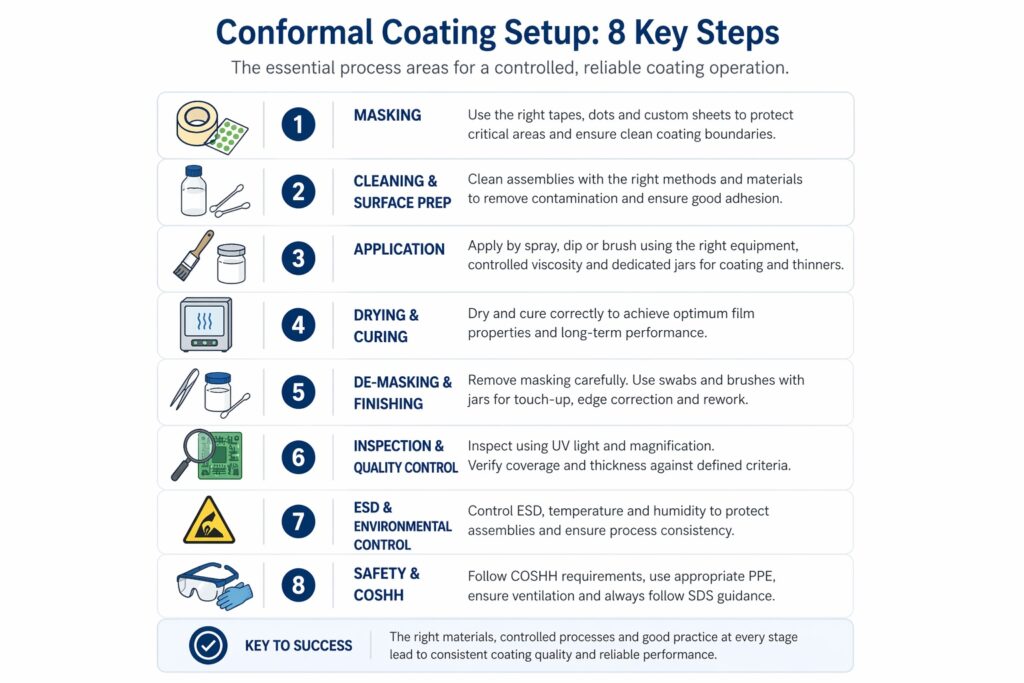
Conformal coating setup process showing the key stages from masking and cleaning through to application, inspection and finishing.
1. Masking: Where Most Coating Problems Begin
Masking is one of the most critical parts of the conformal coating process.
Incorrect masking materials or methods lead directly to:
- Coating ingress into connectors and interfaces
- Excessive rework during de-masking
- Inconsistent coating boundaries
Core masking consumables (correct selection matters)
- High-quality masking tapes designed for conformal coating, clean removal, and low residue risk
- Masking dots supplied in precision die-cut sheets for consistent masking of repeat areas
- Custom masking sheets and die-cut masking shapes for repeatable production masking
Not all tapes, dots, and custom masking sheets are equal. General-purpose masking materials often leave residue, lift during coating, or fail during curing, which creates unnecessary rework and process instability.
If masking is treated as a low-value consumable decision, coating quality usually suffers later in the process.
For masking materials intended for conformal coating applications, see our masking solutions.
Basic tools
- ESD-safe tweezers
- Scalpel
- Cutting mat
- Overhead de-ionisers
- Bench magnification for difficult parts
2. Cleaning & Surface Preparation
Surface preparation is one of the most misunderstood parts of conformal coating.
Assemblies are often assumed to be clean, but handling, storage, and environmental exposure mean surfaces are rarely in a controlled condition at the point of coating.
A simple IPA wipe or open solvent bath is commonly used, but this approach is inconsistent and can:
- Redistribute contamination rather than remove it
- Leave residues behind
- Introduce operator variability
What matters in practice
- A defined, repeatable cleaning method
- Appropriate cleaning chemistry rather than reliance on generic solvents alone
- Control of handling to avoid recontamination before coating
Typical practical approach
- Approved PCB cleaning fluid or a controlled IPA process
- Lint-free wipes for general surface cleaning
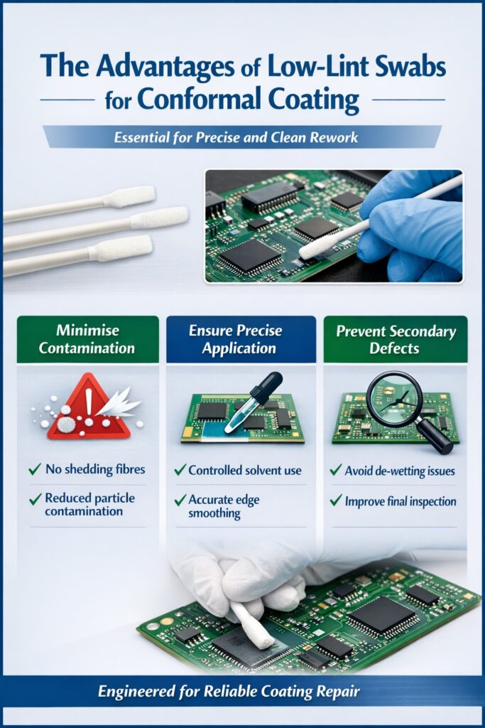
- Polyester swabs for localised, controlled cleaning
Cleaning should be part of the defined process, not treated as a quick preparation step.
A spray booth and a tin of coating do not create a controlled process. The consistency comes from the consumables, handling method, inspection routine, and rework discipline around them.
3. Application: Controlling the Coating Process
Conformal coating can be applied by spraying, dipping, or brushing, but regardless of method, control of the process determines consistency.
Core process items
- Conformal coating material
- Compatible thinners where required
- Mixing containers and stirrers for blending
- Defined viscosity approach
Application setup considerations
- Spray systems, dip tanks, or controlled brush application depending on the process
- Clean, dry air supply for spray systems
- Board handling fixtures or supports
Brush application
Brush coating is widely used for:
- Localised coating application
- Edge definition
- Touch-up during processing
To control this properly, material handling is critical. This includes:
- Dedicated jars for conformal coating to allow small-volume, controlled access
- Separate jars for thinners to avoid cross-contamination
- Controlled decanting rather than working directly from bulk containers
- Using suitable brushes (1/4″ and 1/2″ chisel are ideal) compatible for controlled conformal coating work rather than general workshop brushes
Poor handling leads to contamination, inconsistent viscosity, and unpredictable coating behaviour.
For precision swabs used in controlled coating and touch-up processes, see our polyester swabs.
Process control
- Witness coupons for verifying coating behaviour and coverage
- Consistent loading and handling method
- Defined application parameters rather than operator judgement alone
4. Drying & Curing
Even basic coating systems require controlled drying.
Without this, issues can include:
- Uneven finish
- Extended tack time
- Contamination during cure
Typical setup
- Ambient drying racks
- Drying cabinet or oven depending on the coating system
5. De-Masking & Finishing for Liquid Coatings
For liquid conformal coatings, de-masking and finishing must be controlled to avoid damaging the coating.
Incorrect methods can:
- Lift coating edges
- Tear films
- Leave contamination at boundaries
Controlled approach
- Careful removal of tapes and dots using tweezers
- Use of low-lint polyester swabs to press down lifted coating edges
- Use of low-lint polyester swabs to remove unwanted coating from defined areas where correction is needed
- Controlled use of suitable brushes for edge correction and blending repaired areas
- Dedicated jars for holding small volumes of coating for touch-up
- Dedicated jars for holding thinners for controlled rework and finishing
Rework should be controlled and localised, not improvised using bulk materials or rough tools.
For an example of controlled liquid coating rework, see our Insight on repairing lifted conformal coating edges.
6. Inspection & Quality Control
Inspection confirms whether the process is under control, not just whether coating is present.
Minimum inspection setup
- UV inspection light at 365 nm
- Controlled inspection area
- Magnification for detailed checks
Additional control
- Thickness measurement tools
- Defined inspection criteria
7. ESD & Environmental Control
Electrostatic control and environmental stability influence coating behaviour and reliability.
Typical requirements
- ESD-safe work surfaces
- Grounding and wrist straps
- Controlled humidity where possible
8. COSHH & Safety Requirements
Any coating process introduces chemical handling requirements.
Minimum considerations
- Safety Data Sheets (SDS)
- COSHH assessments
- Appropriate PPE including gloves, eye protection, and respiratory protection where required
- Ventilation such as a spray booth or suitable extraction system
What Most Setups Get Wrong
From experience, the most common issues are:
- Poor masking material selection
- Inadequate or inconsistent cleaning
- Lack of control in application method
- Incorrect rework techniques
- No defined inspection standard
These are not minor issues. They directly affect yield and long-term reliability.
A Practical Starting Point
For teams setting up a new coating process, it is often best to begin with a controlled starter set of consumables rather than attempting to define everything up front.
A typical starting point includes:
- Masking tapes, dots, and custom masking sheets in a practical range of sizes
- Precision cleaning and touch-up consumables such as polyester swabs
- Small-volume handling items such as brushes, and dedicated coating & thinner jars
- Witness coupons for basic process verification
This allows initial trials, after which requirements can be refined based on the actual assemblies being coated.
Next Steps
If you are setting up a conformal coating process and would like guidance on selecting the right consumables or refining your setup after initial trials, SCH can support with:
- Starter consumable packs
- Masking solutions tailored to your assemblies
- Application and rework consumables
- Training and process support
Why This Matters
Conformal coating is not just a material. It is a controlled process. Getting the fundamentals right at the start avoids rework, improves consistency, and reduces long-term cost.
Why Choose SCH Services?
SCH supports customers with practical conformal coating knowledge, process-led guidance, and the consumables needed to get coating operations under control from the start.
Whether you are setting up a new coating process or tightening an existing one, SCH can help you define a more controlled and repeatable approach.
This article provides general technical guidance only. Final process design, material selection, and validation should be confirmed against application-specific requirements, product data, and relevant industry standards.