Practical ways to check wet and dry film thickness on conformal coated PCBs
There are several practical ways to measure conformal coating thickness on a printed circuit board (PCB). Some methods are used on the wet coating before cure, while others are used once the coating has dried or fully cured.
Common options include:
- Non-destructive eddy current systems
- Micrometer screw gauges
- Wet film gauges
This page is a quick practical guide. For a broader engineering review, including wet, dry and optical approaches, see our main article: Conformal Coating Thickness Measurement: Wet, Dry & Optical Methods.
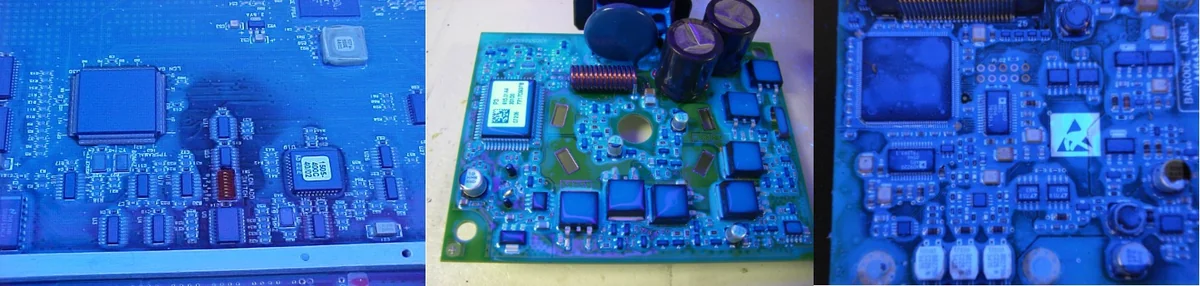
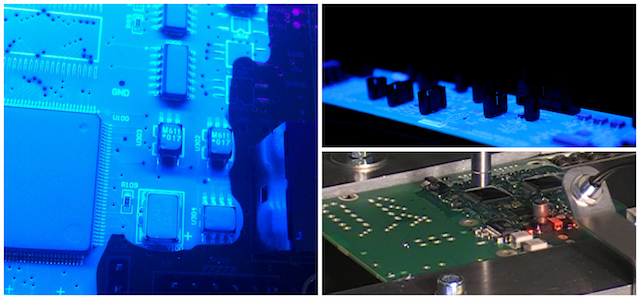
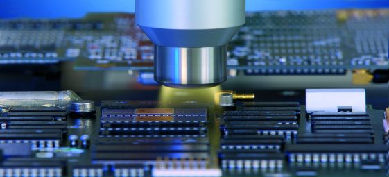
Non-destructive eddy current system
A fast method for measuring coating thickness is an eddy current system. When used correctly, the process can be extremely quick and accurate, with resolution down to approximately ±1 µm depending on the equipment, substrate and test conditions.
Using a gauge and flying probe for measurement is straightforward. The process works by placing the test probe head flat on the surface of the conformal coating. The reading is almost instantaneous and provides a repeatable result for coating thickness measurement.

Using a test probe system like the Positector 6000 can quickly give conformal coating thickness measurements without damaging the circuit board.
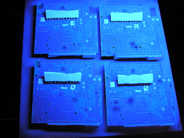
Test coupons are often the ideal way to measure coating thickness, whether the coating is sprayed or dipped, and they can also be retained as a physical production record.
Apply the coating to the test coupons at the same time as the circuit board. This provides a permanent reference and a practical guide to the coating thickness being achieved in the process.
There are some limitations with this type of system:
- There must be conductive metal directly below the measurement point, otherwise the system cannot work correctly.
- There must be a flat area large enough for the test probe. The smallest practical probe is approximately 6 mm in diameter, so very small areas are generally not suitable.
- The surface being measured needs to be flat. Curved or uneven surfaces can introduce errors into the reading.
Micrometer screw gauge
A lower-cost method is to use a calibrated micrometer screw gauge capable of measuring down to around ±10 µm. First, measure a point on the board or test coupon. Then apply the coating, allow it to cure, and measure the same point again. The difference gives the coating thickness.
There are a couple of pitfalls to avoid. Make sure the coating is cured hard enough before measuring, because a soft coating may compact and give a false reading. Also, do not rely on a single point. Take an average of at least three or four readings to improve confidence in the result.
Again, test coupons are usually the best choice for this type of measurement, whether the process is spraying or dipping, because they can be measured consistently and retained as part of the quality record.
Wet film gauge
A final method is wet film measurement, which is simple and cost-effective.
This technique uses a comb gauge with different tooth heights that is placed into the wet coating. The imprint left in the material indicates the wet film thickness. If the solids content of the coating is known, the approximate dry film thickness can then be estimated.

A wet film gauge is a low cost method for measuring coating thickness while the conformal coating is wet. Using the solids content in the material and the wet film thickness allows the dry film thickness to be estimated.
Choosing the right method
- Eddy current is fast and non-destructive, but only works where the board structure and geometry allow it.
- Micrometer measurement is inexpensive and simple, but depends on stable repeatable measurement points and a fully cured coating.
- Wet film gauges are useful during application control, but they estimate dry thickness rather than directly measuring the final cured film.
In practice, the best method depends on whether you are trying to control the process in real time, verify final cured thickness, or create a documented quality record using test coupons.
Related technical guidance
- Conformal Coating Thickness Measurement: Wet, Dry & Optical Methods
- Orange Peel in Conformal Coating
- Conformal Coating Processes Hub
Thickness should not be considered in isolation. Surface profile, coverage, edge definition and defects such as orange peel can all affect how a measured thickness should be interpreted.
Why Choose SCH Services?
SCH Services supports manufacturers with practical coating process control, thickness measurement guidance, defect reduction and production support across conformal coating operations.
If you need help selecting a suitable measurement method, setting up test coupons, or improving process consistency, contact us to discuss your application.
Disclaimer: This article is provided as general technical guidance only. Measurement method suitability, accuracy and acceptance criteria should be validated against the coating material, board design, process conditions and any applicable customer, IPC or internal quality requirements.