
What Nano Coatings Can and Can’t Do on PCB Assemblies
Understanding where nano coatings add real value — and where they do not replace conformal coating
Nano coatings attract attention because they offer very thin, low-build surface treatment with strong hydrophobic behaviour. On the right PCB assembly, that can be extremely useful.
The problem is that nano coatings are often misunderstood. They are sometimes treated as if they are simply a thinner version of conventional conformal coating. They are not. Their behaviour, protection mechanism and limitations are different.
Nano coatings can be highly effective as an enhancement layer, particularly where connectors, tight geometries or mixed coated and uncoated regions are involved. But on their own, they do not replace thicker conformal coatings where stronger dielectric barrier performance or physical protection is required.
Nano coatings make more sense when viewed as part of the wider protection decision between conformal coating, nano coating and Parylene, rather than being treated as a direct replacement for every coating requirement.
Need to compare specific advanced coating options? Use the CytoPel coating selection matrix to compare ultra-thin, hydrophobic, PFAS-free, hard and UV-curable coating routes.
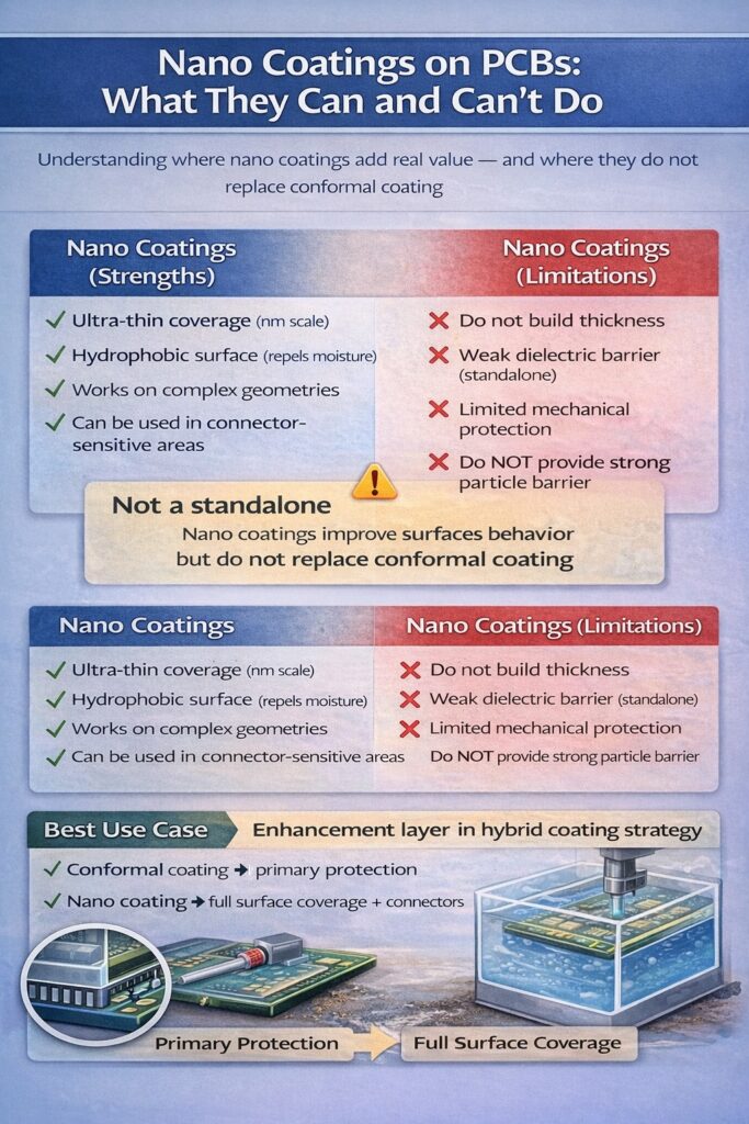
Nano coatings provide ultra-thin hydrophobic coverage and can be used in connector-sensitive areas, but they do not replace conformal coating where dielectric strength, thickness or particle isolation are required.
1) What nano coatings are good at
Nano coatings perform well where the goal is to create a very thin, low-surface-energy layer across difficult or sensitive PCB features.
- They spread easily across complex shapes
- They can cover areas that are difficult to coat conventionally
- They produce hydrophobic surfaces that resist wetting
- They can reduce moisture adhesion and help reduce contamination sticking to the surface
- They can often be used in connector-adjacent areas that cannot tolerate thick coating build-up
This makes them particularly useful where the design demands coverage without heavy build-up.
Where that value depends on water beading, droplet movement or low surface energy, see why some coatings cause water to bead and roll off for a practical explanation of the surface behaviour behind hydrophobic coating performance.
2) Why engineers like them on difficult assemblies
On challenging PCB assemblies, nano coatings can address problems that conventional coatings struggle with.
- Tight geometries where thick coatings can pool or wick
- Connectors and contact-adjacent zones that must remain functional
- Areas where masking complexity becomes excessive
- Assemblies needing a fast, low-build process for broad surface treatment
In these situations, nano coatings can extend surface treatment into places where a conventional coating process is either risky or impractical. These same conditions are often where coating failure originates if not engineered correctly — see Why Conformal Coating Fails in Complex PCB Assemblies.
3) What nano coatings do not do well
Nano coatings are not a direct replacement for conventional conformal coatings. Their main limitations are linked to the same feature that makes them useful: very low film build.
- Very low film thickness – they do not create the same physical barrier as thicker coatings
- Lower dielectric build – they are not the best standalone answer where stronger insulation margin is required
- Limited mechanical protection – they do not protect in the same way against abrasion, handling or local film damage
- Limited defect bridging capability – they do not bury rough surfaces or sharp edges in the way a thicker system can
- Weak standalone protection against conductive particles – they do not provide a strong physical barrier if particle isolation is a key requirement
They are best understood as a surface-function layer, not a heavy-duty barrier coating.
Important: Nano coatings can reduce wetting and contamination adhesion, but they do not provide a strong physical barrier against conductive particles in the same way a thicker conformal coating can.
4) Why “thin” is both the strength and the weakness
The reason nano coatings are attractive is also the reason they are limited.
- Strength: they do not interfere heavily with geometry or contact regions
- Weakness: they do not build enough thickness to behave like a robust conformal barrier
This is why they work well for water repellency and surface enhancement, but should be used more carefully where the design depends on film thickness as part of the protection strategy.
A nano coating may repel water effectively at the surface level, but that does not automatically make it equivalent to a conventional conformal coating. For a deeper explanation, see our guide to hydrophobic conformal coatings.
5) Why nano coatings spread so well
Nano coatings are often based on very low surface energy chemistry. That gives them strong spreading and wetting behaviour across PCB surfaces.
- They can coat fine features very effectively
- They can penetrate tight spaces and difficult regions
- They create highly water-repellent surfaces once cured or dried
That behaviour is a major advantage for coverage, but it also means they are difficult to stop precisely if clean boundaries are required.
That same spreading behaviour is one reason local keep-out control can become difficult in production. For a more detailed look at realistic edge capability, see Selective Conformal Coating Accuracy: Why ±1 mm Is the Reality.
6) Where nano coatings work best on PCB assemblies
Nano coatings are particularly useful where the coating strategy needs broad surface treatment with minimal build rather than heavy barrier thickness.
- Connector-sensitive designs
- Boards with mixed coated and uncoated functional regions
- Hydrophobic enhancement requirements
- Tight geometries where heavy film build causes more problems than benefits
- Assemblies where the main goal is to reduce moisture wetting and reduce contamination adhesion rather than build a heavy barrier layer
Connector behaviour is a key risk area in these designs. For a deeper understanding, see Press-Fit Connectors and Conformal Coating Problems.
This is why they are powerful as part of a system solution, especially in hybrid coating strategies.
Process option: nano coating can be used as a no-mask coating approach where connector geometry, complexity or production constraints make masking impractical, but this should be selected based on acceptable risk rather than assumed protection.
7) Where nano coatings should be treated carefully
Nano coatings should be evaluated more carefully where the application depends on thickness, insulation margin, physical barrier performance or strong local durability.
- The design needs stronger dielectric barrier thickness
- The environment is harsh and long-term barrier performance is critical
- The PCB must tolerate significant handling or mechanical abuse
- The assembly has sharp boundaries where uncontrolled spread creates risk
- The protection strategy assumes the coating itself provides substantial insulation depth
- Conductive particle isolation is a major requirement and a real physical barrier is needed
In these cases, nano coating alone may leave the design under-protected.
8) Particle contamination: where the message is often misunderstood
Particle contamination is one of the areas that causes the most confusion. Nano coatings can help by changing surface behaviour, but they should not be treated as a full physical barrier.
Nano coatings can help by:
- Creating a hydrophobic surface
- Reducing wetting
- Making it harder for some contamination to adhere strongly to the surface
But nano coatings do not provide a strong standalone physical barrier against conductive particles in the same way a thicker conformal coating can.
Where particle-related shorting risk is significant, nano coating is usually best treated as an enhancement layer within a broader process strategy, not as the sole protective answer.
This is one reason contamination-sensitive assemblies often need a broader process strategy rather than a single material decision. See Why Conformal Coating Fails in Complex PCB Assemblies.
Sequence matters: if nano coating is used in a combined process, it should normally be applied after conventional conformal coating, not before it.
9) Why sequence matters if nano is combined with other coatings
Nano coatings should normally be applied after the conventional conformal coating stage.
- Apply conformal coating first where primary protection is needed
- Leave sensitive or connector-critical areas free from thick coating
- Apply nano coating second as the full-board enhancement layer
If nano coating is applied first, its hydrophobic nature can interfere with wetting and adhesion of later liquid coatings.
Used this way, nano coating becomes part of a hybrid coating strategy rather than a standalone solution.
10) The best way to think about nano coatings
The most useful engineering view is this: nano coatings are not “better conformal coatings”. They are different tools with different strengths.
They are excellent when you need:
- Thin coverage
- Hydrophobic behaviour
- Surface-function improvement
- Reduced moisture wetting and reduced contamination adhesion
- Treatment in connector-sensitive zones
They are weaker when the application depends on thickness, barrier depth, mechanical robustness or strong standalone particle isolation.
11) Key conclusion
Nano coatings can add major value on PCB assemblies, but only when their limits are understood clearly.
They are highly effective as a thin, hydrophobic, full-coverage enhancement layer. They are much less effective when treated as a direct substitute for thicker conformal coatings in applications needing stronger insulation, physical barrier performance or robust standalone protection against conductive particles.
Used correctly, they are powerful. Used in the wrong role, they create false confidence.
Related process articles
Use Nano Coatings in the Right Role
Nano coatings are powerful when used correctly — but they are not a direct replacement for conformal coating. The key is understanding where they add value, and where they introduce risk.
🔍 Not sure if nano coating is enough?
If your application involves moisture protection, electrical insulation or harsh environments, nano coating alone may not provide sufficient protection.
🧠 Considering a hybrid approach?
Many complex assemblies benefit from combining conformal coating with nano coating — using each where it performs best.
🔧 Need help defining the right protection strategy?
If you are unsure how nano coating fits into your application, SCH can help define a realistic coating approach based on geometry, environment and process capability.
SCH Services supports coating selection, hybrid strategy development and production implementation — ensuring nano coatings are used where they genuinely improve performance.
📞 Call: +44 (0)1226 249019 | ✉ Email: sales@schservices.com
Note: This article provides general technical guidance only. Final coating strategy, material selection, safety and compliance decisions must be verified by the product manufacturer and validated against the applicable standards and qualification tests.
