
Where plasma-deposited nano films fit in surface engineering and electronics protection
Plasma coating is a surface treatment process in which a reactive coating precursor is introduced into a plasma and deposited onto a substrate as an ultra-thin functional film. It is typically used where very low film thickness, tailored surface behaviour or specialist adhesion performance is required.
In practical terms, plasma coating is not the same as traditional conformal coating and it is not the same as Parylene deposition. It belongs more to the world of surface engineering, where the goal is often to modify how a surface behaves rather than build a thick physical barrier.
That makes plasma coating interesting, but also easy to misunderstand. The key question is not whether it is advanced, but where it actually fits and what problems it is designed to solve.
How plasma coating works
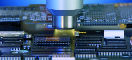
In a plasma coating process, a precursor material is introduced into a plasma zone, often through a jet nozzle or controlled gas-phase system. The plasma activates the chemistry, increasing its reactivity and allowing it to bond to the substrate surface more effectively.
This process can be adjusted for different materials including metals, glass, ceramics and plastics. Depending on the chemistry used, the resulting film can be tailored to create different surface properties such as water repellence, improved adhesion or barrier enhancement.
Because the film is extremely thin, plasma coating is usually used to change surface function rather than build the kind of thick protective layer associated with conventional conformal coatings.
Important: Plasma coating should not be confused with plasma surface preparation. Plasma preparation activates or cleans a surface before coating, while plasma coating deposits a functional film onto the surface itself.
What plasma coatings can do
Plasma-deposited coatings are typically used to alter surface behaviour in a very targeted way. Depending on the chemistry and process design, they can be made hydrophobic or hydrophilic and can improve how a surface performs in later manufacturing or service.
- Barrier improvement for selected plastic or functional surfaces
- Adhesion improvement for bonding or paint application
- Release properties for tooling and mould-related applications
- Corrosion resistance support where ultra-thin barrier behaviour is beneficial
- Surface energy modification to improve how a material interacts with liquids, adhesives or later coatings
These are specialist functions. They are not direct equivalents to the role of a conventional PCB conformal coating.
Where plasma coating fits in electronics
In electronics, plasma coating is best understood as a niche or specialist surface engineering option rather than a mainstream replacement for conformal coating. It may be relevant where very thin deposited functionality is needed, but it does not automatically replace the insulation, thickness or physical protection provided by traditional coating systems.
That is why it is important to compare it in the right way. If the real need is full electrical insulation, environmental barrier performance or robust film build, then conventional conformal coatings or Parylene may still be the more appropriate technologies.
For a broader comparison of established protection strategies, see Parylene vs Conformal Coating: How to Choose the Right Protection for Electronics.
What plasma coating does not replace
Plasma coating is often interesting because it is thin, highly engineered and flexible at surface level. But those same features also mean it should not be overstated.
- It does not automatically replace conformal coating where thickness and dielectric protection are required
- It does not automatically replace Parylene where true conformal vapour-deposited coverage is needed
- It does not remove the need for proper process selection, testing and validation
Like other advanced thin-film technologies, it is best viewed as a specialist tool for specific problems rather than a universal answer.
Reality check: If the requirement is mainstream PCB protection in a harsh environment, plasma coating is usually not the first question to ask. The first question is what level of barrier, insulation, coverage and process control the product actually needs.
Final perspective
Plasma coating is a legitimate and highly specialised surface engineering technology. Its value lies in controlled surface modification, ultra-thin deposited functionality and application-specific performance tuning.
For most electronics users, the important thing is understanding where it fits relative to better-known technologies such as conformal coating and Parylene. The goal is not to use the most advanced process available, but to select the process that matches the product, environment and manufacturing reality.
If you are trying to choose between different protection strategies, it is usually better to start with the function required and then work back to the most appropriate coating technology.
Need help reviewing a coating or surface protection problem?
SCH supports customers with coating selection, process review and technical guidance across conformal coating, Parylene and specialist protection strategies.
Contact us to discuss your application.
