Mon - Thur 7.30-15.30   Fri 7.30-14.00

Are there design rules for applying conformal coatings?


Conformal coating is not simply a consumable material. Unfortunately, for too many designers, conformal coating is simply a part number, to be applied to circuit boards. However, this can be a major problem especially in the conformal coating production stage of the process.

There are guidelines in the IPC standards that may help with Design for Manufacture (DFM) principles. These are worth considering. Unfortunately, there are no official design guidelines that will help directly with the application process and conformal coating.

Conformal coating treated as a part number rather than a design consideration can cause production issues

When conformal coating is treated as a simple part number rather than a design consideration, it can create significant problems during the production stage.

Conformal Coating Design Hub

SCH Services Ltd has developed design rules for conformal coating in their Design Hub to help users get the fundamentals right.

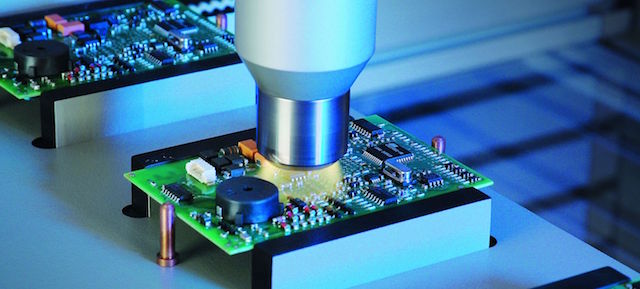
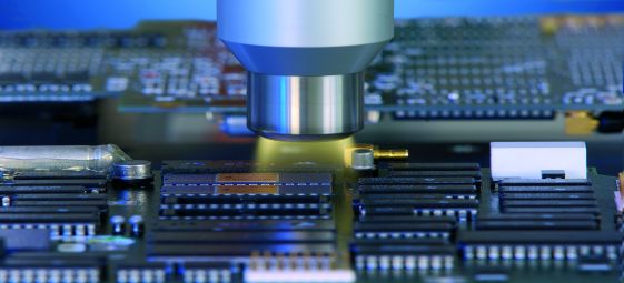
The hub focuses on designing PCBs and assemblies for coating, including keep-out zones, component spacing, creepage and clearance, and applying DfM/DfCC principles before manufacture. The philosophy is that for companies embracing lean philosophies and applying conformal coatings, a failure to appreciate the subtleties of the application process can result in an un-coatable (at least as specified) assembly process.

The problem is if the rules are not followed, the resultant circuit board design can challenge even the most sophisticated conformal coating system and its operator to achieve the finish desired.

For further information visit conformal coating design rules to learn more.


Need Process Support?

Optimising electronics coating methods requires the right combination of materials, equipment, and operator training. Partner with SCH Services for:

Infographic explaining whether MIL-SPEC qualification is required for conformal coating and how legacy MIL-I-46058C references relate to modern standards.

Do you need MiL spec qualification for your conformal coating?


A common question from aerospace and defence customers is: β€œDo we need MIL-SPEC qualification for our conformal coating?”

The short answer is: sometimes β€” but only when it is contractually required.

Confusion usually arises because legacy military standards are still referenced on drawings, purchase orders, or coating datasheets, even though the underlying standards landscape has changed.

For a full explanation of how military (MIL) requirements relate to modern conformal coating standards, see: MIL-I-46058C (Cancelled) & MIL Standards for Conformal Coating
.


When is MIL-SPEC actually required?

In practice, manufacturers usually know they require MIL-related compliance when:

  • The product is for a military or defence programme
  • MIL requirements are explicitly called up on the customer drawing
  • The purchase order or contract includes MIL flow-down requirements

If none of these are present, β€œMIL-SPEC” is often being used as shorthand for high reliability rather than a defined manufacturing requirement. This is where misunderstandings commonly occur.


Be cautious with datasheets claiming β€œmeets MIL-I-46058C”

Many conformal coating datasheets state that the material β€œmeets the requirements of MIL-I-46058C”. This wording should be treated with caution.

MIL-I-46058C is a cancelled standard, and simply stating compliance does not mean the coating has been independently approved or qualified. In many cases, the claim refers only to internal or historical test data.

Where defence programmes genuinely require MIL-style material qualification, customers will often expect evidence beyond a datasheet statement.


What is the Qualified Product List (QPL)?

Historically, conformal coatings tested against MIL-I-46058C were listed on the Qualified Product List (QPL).

The MIL-I-46058C Conformal coating standard has been inactive for new designs since the late 1990s, but QPL listings are still referenced in legacy documentation and long-lifecycle programmes.

Coatings appearing on the QPL would have undergone independent third-party testing rather than self-certification. This is an important distinction.

However, the presence (or absence) of a coating on the QPL does not automatically determine its suitability for modern programmes. What matters today is how customer requirements are defined and verified.


What is normally used instead today?

Modern defence and aerospace programmes typically rely on a combination of:

  • IPC-CC-830 for conformal coating material performance and qualification
  • IPC-A-610 for workmanship and acceptance criteria
  • Customer drawings and specifications defining coverage, keep-out zones and inspection evidence

MIL requirements are therefore usually met through industry standards plus contractual flow-downs, rather than through a single active β€œMIL-SPEC” document.


Need to understand how the standards fit together?

The Conformal Coating Standards Hub brings together SCH’s guidance on IPC-A-610, IPC-CC-830, IEC 60664, UL 746, NASA workmanship standards and how they relate to conformal coating and Parylene.

It is designed to help engineering, quality and procurement teams understand:

  • What each standard actually covers
  • How acceptance, material qualification and inspection requirements interact
  • Where legacy MIL references still appear β€” and how to interpret them safely

You can also explore related hubs covering Design, Inspection & Quality and Parylene Coating.


If you need help interpreting customer requirements, legacy MIL references, or selecting compliant coating materials and inspection criteria, contact SCH Services.

πŸ“ž Call: +44 (0)1226 249019 Β | βœ‰ Email: sales@schservices.com

What is Plasma Cleaning?


Plasma cleaning is a process of using plasma energy to clean and modify the surface of a substrate like a circuit board assembly. It is a highly effective surface cleaning and treatment process before application of conformal coatings and Parylene and is gaining more popularity due its highly effective performance.

Plasma cleaning is a process of using plasma energy to clean and modify the surface of a substrate like a circuit board assembly. It is a highly effective surface cleaning and treatment process before application of conformal coatings and Parylene.

What is Plasma?

Plasma is the energy-rich gas state (also known as the fourth state of matter) that can be used to modify the surface of a product to improve its performance.

Plasma technology is based on a simple physical principle. Matter changes its state when energy is supplied to it. Solids become liquid. Liquids become gas. If additional energy is then fed into a gas by means of electrical discharge it eventually ionises and goes into the energy-rich plasma state, plasma is created.

This modification can be improving the adhesion of a conformal coating or change the surface characteristics of the board.


How is Plasma used for improving the performance of coatings with printed circuit boards?

For electronic circuit surfaces, plasma treatment can be used in two highly effective ways.

That is it can:

  • Clean the surface of the circuit board. The surface will be free of residues and 100% contamination free including release agents and additives.
  • Activate the surface of the circuit board assembly. This will allow easier bonding and better adhesion of conformal coatings and Parylene.

These properties make it an interesting technique for improving the surface performance of an electronic circuit board.

In fact, plasma treatment can clean, activate or coat nearly all surfaces. These surfaces include plastics, metals, (e.g., aluminum), glass, recycled materials and composite materials. This means the plasma process can be highly effective on many different products.


How is the plasma applied to a circuit board to clean and activate the surface?

For materials like liquid conformal coatings and Parylene then atmospheric pressure plasma is an excellent process for cleaning surfaces and improving adhesion and surface energy performance of circuit boards.

Atmospheric plasma is generated under normal pressure. This means that low-pressure chambers are not required. The plasma is created with clean and dry compressed air and does not require forming gases. It is possible to integrate plasma directly into manufacturing processes under normal pressure conditions.

Typical plasma components used for cleaning surfaces on circuits are:

  • Plasma jets (nozzles) to apply the plasma to the surface of the circuit board. They could be controlled by a robotic system.
  • The plasma generators that create the plasma to clean or supply the coatings as required. They provide output power and, in conjunction with complete pretreatment stations, assume various control functions.
  • The process monitoring that controls the nozzles, the movement of the system and the quality of the output.

These three parts form the plasma cleaning process.


Want to know more about plasma cleaning and conformal coating performance?

Contact us now to discuss what we can do to help. Or, give us a call at (+44) 1226 249019 or email your inquiries at sales@schservices.com

Cleaning No-Clean Flux Residues for Conformal Coating Reliability


Why incomplete cleaning can lead to adhesion loss, corrosion and long-term coating reliability problems

Cleaning the residues left behind by a no-clean flux process is one of the most difficult and misunderstood stages of PCB preparation. These residues are specifically designed to remain on the board, so they are not formulated to be removed easily.

That becomes important when conformal coating is planned. Surface contamination, partially removed residues and poorly matched cleaning chemistry can all affect wetting, adhesion and long-term reliability. The goal is not simply to make the board look cleaner. The goal is to avoid creating a worse failure mechanism than the original residue itself.

Cleaning PCB residues before conformal coating

How do you clean no-clean flux residues if you need to?

Whether a no-clean flux residue can be cleaned effectively depends on the cleaning chemistry’s saponification factor and its compatibility with the residue chemistry present on the assembly.

Saponification is the ability of the cleaning chemistry to soften and break down the residue so it can be dissolved and removed. In simple terms, the more effectively the chemistry attacks the residue, the easier it becomes to clean the surface properly.

The key requirement is complete removal. If the cleaning chemistry does not fully dissolve and remove the residue, the process may create more risk rather than less.

Reality check: A partially cleaned no-clean residue may be more dangerous than a residue left untouched, because the protective resin matrix can be disturbed without fully removing the active chemistry beneath it.

What happens if the residues are only partially dissolved?

A no-clean residue that is only partly cleaned away may be far worse for a printed circuit board assembly than a no-clean residue left untouched. One reason is that lead-free flux activators are generally more active than those used in earlier leaded formulations.

When the residue is left in place, the activators are held within the carrier resin matrix. At normal operating temperatures, that matrix helps keep the residue stable and reduces the risk of corrosion-related problems.

However, if the protective matrix is only partly removed by an inadequate cleaning process, the active chemistry may become exposed. This can initiate corrosion on the circuit board and may be accelerated by heat, electrical bias in service or high relative humidity.

Why this matters for conformal coating

Conformal coating is often applied to improve environmental protection and long-term reliability. But coating over contamination or marginally cleaned residues can lock defects into the assembly rather than eliminate them.

If cleaning is incomplete, the result may include poor coating wetting, reduced adhesion, localised dewetting, corrosion risk and reliability problems that only appear later in service.

This is why cleaning should be treated as a controlled process step, not as a cosmetic operation. If you are reviewing coating failures, it is also worth understanding how poor preparation interacts with broader process issues covered in our article on why conformal coating fails in complex PCB assemblies.

So how should no-clean residues be assessed?

When considering whether to clean no-clean residues before coating, three questions matter:

  1. Can the residue actually be cleaned effectively on this assembly?
  2. Have you matched the cleaning chemistry to the degree of difficulty and the available cleaning process?
  3. Have you validated the overall process by testing, rather than assumption?

These questions matter because no-clean fluxes vary, assemblies vary and cleaning processes vary. A workable answer on one product may fail on another. Validation is essential.

Why Choose SCH Services?

SCH Services supports conformal coating users with practical process knowledge, coating services, training and engineering support. If you are reviewing cleaning, coating adhesion or broader process reliability, we can help assess the issue in the context of the full coating process rather than as an isolated symptom.

To discuss cleaning, coating preparation or process troubleshooting, contact us or call (+44) 1226 249019.

↑ Back to top

This article is provided as general technical guidance only. Cleaning chemistry, residue behaviour and conformal coating performance vary by assembly, flux system and process conditions. Final process decisions should be validated through suitable trials, inspection and reliability testing.

FAQs Atomic Layer Deposition (ALD)


Atomic Layer Deposition (ALD) is an advanced thin-film coating technology used where extreme thickness control, conformality, and film integrity are required at the nanometre scale. It is increasingly specified for high-reliability electronics, semiconductor devices, optics, energy systems, and biomedical components where conventional coating methods reach their technical limits.

Unlike liquid-applied coatings or conventional vapour deposition processes, ALD builds coatings one atomic layer at a time through a self-limiting surface reaction. This allows engineers to precisely define film thickness, composition, and uniformityβ€”even on complex 3D structures, high-aspect-ratio features, and densely packed devices.

The Atomic Layer Deposition FAQs below provide a practical overview of:

  • What ALD is and how it differs from other CVD-based coating processes
  • The types of materials that can be deposited using ALD
  • How the ALD process works in practice
  • Where ALD is typically used across different industries
  • The key advantages and limitations of ALD compared with alternative coating technologies

This section is intended to give engineers, designers, and procurement teams a clear understanding of when ALD is technically justified and how it fits alongside other advanced coating solutions such as Parylene and liquid conformal coatings.

What is ALD?

Atomic Layer Deposition (ALD) belongs to the family of Chemical Vapour Deposition methods (CVD).

  • It is a deposition process at a nano-scale level within an enclosed vacuum chamber.
  • The deposition process forms ultra-thin films (atomic layers) with extremely reliable film thickness control.
  • This provides for highly conformal and dense films at extremely thin layers (1-100nm).

What coatings are deposited in ALD?

ALD principally deposits metal oxide ceramic films. These films range in composition from the most basic and widely used aluminum oxide (Al2O3) and titanium oxide (TiO2) up to mixed metal oxide multilayered or doped systems.

How does ALD work in practice?

The ALD deposition technique is based upon the sequential use of a gas phase chemical process.

  • Gases are used to grow the films onto the substrate within a vacuum chamber.
  • The majority of ALD reactions use two chemicals called precursors.
  • These precursors react with the surface of a material one at a time in a sequential, self-limiting, manner.
  • Through the repeated exposure to alternating gases there is a build up of a thin coating film.

Where is ALD used?

ALD is used in many different areas including:

  • Micro-electronics
  • Semiconductors
  • Photovoltaics
  • Biotechnology
  • biomedical
  • LEDs
  • Optics
  • Fuel cell systems

What are the Advantages and disadvantages of ALD

Advantages

  • Self-Limiting. The ALD process limits the film thickness. Many other processes like Parylene are dependent upon amount of dimer and will continue to deposit successive polymer layers until it is completely used up.
  • Conformal films. ALD film thickness can be uniform from end to end throughout the chamber. Other coatings like Parylene can have a varied coating thickness across the chamber and the devices being coated.
  • Pinhole free. ALD films can be pinhole-free at a sub-nanometer thickness. Parylene and some other materials are only pinhole-free at micron levels.
  • ALD allows layers or laminates. Most other films including Parylene are single component layers.

Disadvantages

  • High purity substrate. This is very important to the quality of the finish similar to many other vapour deposition processes.
  • ALD Systems can range anywhere from $200,000 to $800,000 based on the quality and efficiency of the instrument. This tends to be 3-4 times the prices of a Parylene system.
  • Reaction time. Traditionally, the process of ALD is very slow and this is known to be its major limitation.
  • Masking challenges. The ALD masking process must be perfect. Any pinhole in the masking process will allow deposition beyond the masking barrier.

What are some of the ALD coatings that can be deposited?

A wide variety of chemistries are possible with Atomic Layer Deposition. They include oxides, nitrides, metals, carbides and sulfides.

Want to know more about Atomic Layer Deposition (ALD) coatings?

Contact us now, call us on +44 (0) 1226 249019 or email your requirements on sales@schservices.com

Hybrid ALD/CVD Coatings for LED Protection – Where Do They Really Fit?


Understanding the role of ultra-thin coatings in LED protection without the hype

Protecting LEDs from long-term exposure to harsh environments is becoming increasingly critical, particularly for outdoor and high-reliability applications. Moisture, salt, UV exposure and thermal cycling all create failure risks that must be managed through coating selection.

There are already multiple established protection strategies including Parylene, liquid conformal coatings, ultra-thin fluoropolymers and encapsulation. Each offers advantages, but all involve trade-offs between protection level, process complexity, optical performance and cost.

Hybrid ALD (Atomic Layer Deposition) / CVD (Chemical Vapour Deposition) coatings are often presented as a new alternative. The key question is not whether they are interesting, but where they realistically fit alongside existing coating technologies.

What is a Hybrid ALD/CVD Coating?

Hybrid coatings combine two thin-film deposition techniques into a layered structure.

  • CVD (used in Parylene) deposits a conformal coating in a vacuum environment
  • ALD deposits extremely thin, controlled layers at atomic scale

In hybrid systems, these layers are applied sequentially to build a multi-layer film. The structure is fundamentally different from traditional coatings, as properties can be engineered layer-by-layer rather than relying on a single material.

The result is an ultra-thin coating system, typically in the nanometre range, with tailored barrier, adhesion and surface properties.

Compare this with traditional coating approaches β†’

Why is this approach relevant for LEDs?

LED protection introduces constraints that are not always present in standard PCB coating.

  • Optical clarity – coatings must not reduce light output
  • UV stability – long-term outdoor exposure
  • Moisture resistance – prevention of corrosion and failure
  • Thermal stability – cycling and elevated temperatures

Hybrid coatings are often positioned as suitable because they are extremely thin, highly transparent and can provide good barrier performance relative to thickness.

In applications where traditional coatings create optical or masking challenges, this type of approach becomes more attractive.

Masking Reduction – Not Elimination

One of the most common claims is that hybrid coatings do not require masking due to their extremely low thickness.

Reality check: Ultra-thin coatings can reduce masking requirements, but they do not remove interface risks completely. Connectors, contact surfaces and critical electrical interfaces still require validation.

Whether masking can be reduced depends on:

  • Connector design and contact force
  • Electrical sensitivity of interfaces
  • Long-term wear and fretting behaviour
  • Customer acceptance criteria

In practice, masking strategy becomes an engineering decision rather than being eliminated entirely.

Performance Compared to Established Coatings

Hybrid coatings are often compared with Parylene and liquid conformal coatings. The comparison is not simply performance-based, but application-dependent.

  • Hybrid coatings – ultra-thin, optically clear, engineered film structure
  • Parylene – proven barrier performance and long-term reliability
  • Liquid coatings – scalable, robust and well understood processes

Hybrid coatings can offer advantages in specific LED applications, particularly where optical performance is critical. However, established coatings still dominate in many applications due to proven reliability and process maturity.

The decision is not which coating is β€œbest”, but which is most appropriate for the application and risk profile.

Process and Cost Considerations

Hybrid ALD/CVD processes are often described as low cost due to reduced masking and simple operation. However, real cost depends on the full system.

  • Equipment investment and process control requirements
  • Throughput and batch size limitations
  • Cycle time and scalability
  • Validation and qualification requirements

While operator interaction may be simple, the overall process must be evaluated at production scale rather than individual step level.

For surface preparation prior to coating, see plasma cleaning for conformal coating, which explains how plasma is used to improve adhesion and surface energy.

Where Hybrid Coatings Actually Fit

From a practical engineering perspective, hybrid ALD/CVD coatings are best positioned as a specialist solution rather than a universal replacement.

  • Suitable for optically sensitive applications such as LEDs
  • Useful where ultra-thin coatings provide a design advantage
  • Complementary to existing coating technologies

For most applications, coating selection remains driven by environment, geometry, process capability and reliability requirements.

In many cases, structured coating strategies using established materials remain the most robust approach.

Final Perspective

Hybrid ALD/CVD coatings represent a technically interesting development, particularly for LED protection where optical and environmental requirements must be balanced.

However, they should be viewed as part of a broader coating strategy rather than a direct replacement for Parylene or conformal coatings.

The key is selecting the right coating approach for the application, not chasing a single β€œbest” material.

Need support selecting the right coating approach?

SCH supports coating selection, process design and validation across conformal coatings, Parylene and hybrid strategies.

Contact us to discuss your application.

↑ Back to top

Note: This article provides general technical guidance only. Final design, safety and compliance decisions must be validated against application requirements and relevant standards.

What are conformal coating masking boots and how can they save you money?


The use of masking materials such as tapes, dots and liquid latex can be a highly effective process in protecting components from ingress of conformal coating. However, the masking process can be labour intensive, difficult and time consuming.

Using reusable, custom masking boots offers a labour saving alternative in both the masking and de-masking stages of the coating process. This can save you lots of time and money.

Conformal coating masking boots used on Printed circuit board as an alternative to masking tapes

Three simple reasons why conformal coating masking boots can save you money

  • Masking time is reduced. Using masking boots as an alternative can be 4-5 times quicker than masking tape.
  • De-masking time is reduced. Again it is much quicker to remove masking boots than tape
  • Masking boots don’t leak as easily as tape. So there is less chance of a need to repair or remove leaked coating.

This means you can save a lot of money very quickly when switching to custom masking boots.


How Diamond MT saved nearly 60% of their process time switching to masking boots

Diamond MT, a conformal coating and Parylene coating service provider, found they saved 60% of their current costs by switching to the SCH range of conformal coating masking boots.

Sean Horn, Diamond MT, explains how they did it.

β€œWe had initially wanted to try SCH’s conformal coating masking boots for price savings. However, once we began to work with Lee on our specific masking application, we realised that we could extend the life of our boots over 200%. We switched immediately!

We then realised the importance of working with someone who understands conformal coatings. We will not being going back to our previous supplier.”

Sean Horn, Director, Diamond MT, Parylene and conformal coating subcontract service provider.


Request Your Free Masking Sample Pack

You can experience the quality of our masking solutions first-hand by requesting a free sample pack. The pack includes a selection of our masking tapes, dots, boots and pre-cut shapes, allowing you to test their performance directly in your coating process. It’s a quick and risk-free way to see how our materials ensure clean removal, precise coverage, and time-saving application.

πŸ‘‰ Contact us today to request your free sample pack and find the right masking solution for your production needs.


Find out how much you can save by switching to custom boots

We are happy to provide a quotation for our masking boots so you can see for yourself how much you can save.

Just provide us with three pieces of information:

  • Provide a picture of the board you wish to test
  • Identify the components you need to mask
  • Provide the component identification codes (manufacture details etc)

Contact us today to request your quotation for conformal coating masking boots. Call us on +44 (0) 1226 249019, email your requirements on sales@schservices.com

What is Plasma Coating?


Where plasma-deposited nano films fit in surface engineering and electronics protection

Plasma coating is a surface treatment process in which a reactive coating precursor is introduced into a plasma and deposited onto a substrate as an ultra-thin functional film. It is typically used where very low film thickness, tailored surface behaviour or specialist adhesion performance is required.

In practical terms, plasma coating is not the same as traditional conformal coating and it is not the same as Parylene deposition. It belongs more to the world of surface engineering, where the goal is often to modify how a surface behaves rather than build a thick physical barrier.

That makes plasma coating interesting, but also easy to misunderstand. The key question is not whether it is advanced, but where it actually fits and what problems it is designed to solve.

Plasma treatment of the surface of a circuit board before conformal coating

How plasma coating works

In a plasma coating process, a precursor material is introduced into a plasma zone, often through a jet nozzle or controlled gas-phase system. The plasma activates the chemistry, increasing its reactivity and allowing it to bond to the substrate surface more effectively.

This process can be adjusted for different materials including metals, glass, ceramics and plastics. Depending on the chemistry used, the resulting film can be tailored to create different surface properties such as water repellence, improved adhesion or barrier enhancement.

Because the film is extremely thin, plasma coating is usually used to change surface function rather than build the kind of thick protective layer associated with conventional conformal coatings.

Important: Plasma coating should not be confused with plasma surface preparation. Plasma preparation activates or cleans a surface before coating, while plasma coating deposits a functional film onto the surface itself.

What plasma coatings can do

Plasma-deposited coatings are typically used to alter surface behaviour in a very targeted way. Depending on the chemistry and process design, they can be made hydrophobic or hydrophilic and can improve how a surface performs in later manufacturing or service.

  • Barrier improvement for selected plastic or functional surfaces
  • Adhesion improvement for bonding or paint application
  • Release properties for tooling and mould-related applications
  • Corrosion resistance support where ultra-thin barrier behaviour is beneficial
  • Surface energy modification to improve how a material interacts with liquids, adhesives or later coatings

These are specialist functions. They are not direct equivalents to the role of a conventional PCB conformal coating.

Where plasma coating fits in electronics

In electronics, plasma coating is best understood as a niche or specialist surface engineering option rather than a mainstream replacement for conformal coating. It may be relevant where very thin deposited functionality is needed, but it does not automatically replace the insulation, thickness or physical protection provided by traditional coating systems.

That is why it is important to compare it in the right way. If the real need is full electrical insulation, environmental barrier performance or robust film build, then conventional conformal coatings or Parylene may still be the more appropriate technologies.

For a broader comparison of established protection strategies, see Parylene vs Conformal Coating: How to Choose the Right Protection for Electronics.

What plasma coating does not replace

Plasma coating is often interesting because it is thin, highly engineered and flexible at surface level. But those same features also mean it should not be overstated.

  • It does not automatically replace conformal coating where thickness and dielectric protection are required
  • It does not automatically replace Parylene where true conformal vapour-deposited coverage is needed
  • It does not remove the need for proper process selection, testing and validation

Like other advanced thin-film technologies, it is best viewed as a specialist tool for specific problems rather than a universal answer.

Reality check: If the requirement is mainstream PCB protection in a harsh environment, plasma coating is usually not the first question to ask. The first question is what level of barrier, insulation, coverage and process control the product actually needs.

Final perspective

Plasma coating is a legitimate and highly specialised surface engineering technology. Its value lies in controlled surface modification, ultra-thin deposited functionality and application-specific performance tuning.

For most electronics users, the important thing is understanding where it fits relative to better-known technologies such as conformal coating and Parylene. The goal is not to use the most advanced process available, but to select the process that matches the product, environment and manufacturing reality.

If you are trying to choose between different protection strategies, it is usually better to start with the function required and then work back to the most appropriate coating technology.

Need help reviewing a coating or surface protection problem?

SCH supports customers with coating selection, process review and technical guidance across conformal coating, Parylene and specialist protection strategies.

Contact us to discuss your application.

↑ Back to top

Note: This article provides general technical guidance only. Final design, process and compliance decisions must be validated against the actual substrate, coating chemistry and application requirements.

The ABCs of Plasma Cleaning for Conformal Coating


How plasma treatment improves adhesion, surface energy and coating reliability

Surface condition is one of the biggest drivers of coating success or failure.

Even when the correct conformal coating is selected, poor adhesion, dewetting and long-term reliability issues often trace back to contamination or low surface energy at the substrate level.

Plasma cleaning provides a controlled way to remove contamination and modify surface energy before coating. It is widely used where conventional cleaning alone cannot deliver consistent adhesion β€” particularly for difficult substrates and high-reliability applications.

Emerging ultra-thin coating technologies such as hybrid ALD/CVD coatings reduce reliance on traditional masking and surface preparation, but still depend on controlled surface conditions to perform reliably.

Plasma cleaning infographic showing contamination removal, increased surface energy and improved wetting for conformal coating adhesion on PCB assemblies

Plasma cleaning improves coating adhesion by removing contamination and increasing surface energy, enabling uniform wetting and reliable conformal coating performance on PCB assemblies.

What is plasma?

Plasma is often described as the fourth state of matter. When sufficient energy is applied to a gas, it becomes ionised, forming an ΰ€Šΰ€°ΰ₯ΰ€œΰ€Ύ-rich environment containing ions, electrons and reactive species.

This reactive environment allows plasma to interact with surfaces at a molecular level.

In coating processes, plasma is used to clean, activate or modify surfaces without mechanical contact or liquid chemistry.

Why plasma cleaning is used before conformal coating

Plasma treatment addresses two key challenges in coating processes:

  • Removal of contamination – including organic residues, oils, additives and weak surface films
  • Surface activation – increasing surface energy to improve coating wetting and adhesion

This is particularly important where coatings struggle to wet or bond consistently. For the wider context of how cleanliness affects coating reliability, see surface preparation and cleanliness for conformal coating.

Reality check: Plasma does not fix poor process control. If contamination levels are inconsistent or excessive, plasma may improve results but will not stabilise an unstable upstream process.

What plasma does to a PCB surface

When applied to electronic assemblies, plasma treatment can:

  • Remove organic contamination at a molecular level
  • Increase surface energy to improve wetting
  • Promote stronger adhesion between coating and substrate
  • Enable bonding on otherwise difficult materials

This makes it particularly useful for Parylene processes and difficult-to-bond substrates where adhesion is a known risk.

Types of plasma processes used

There are three main plasma approaches used in surface treatment:

  • Low-pressure plasma: Vacuum-based systems used for high control and uniform treatment. Often used in conjunction with vapour deposition processes such as Parylene.
  • Atmospheric plasma: Operates at normal pressure using compressed air. Easier to integrate inline and widely used for PCB surface activation.
  • Corona treatment: Primarily used for films and packaging materials. Generally not suitable for complex PCB assemblies.

Atmospheric plasma is typically the most practical option for conformal coating processes due to ease of integration and process flexibility.

How plasma is applied in practice

A typical plasma treatment system consists of:

  • Plasma jet or nozzle: directs the plasma onto the PCB surface
  • Generator: creates and controls the plasma energy
  • Motion system: ensures consistent coverage across the assembly
  • Process control: manages power, exposure time and repeatability

These systems are often integrated into automated lines or used as standalone pre-treatment steps.

Where plasma cleaning fits in the process

Plasma is not a universal requirement. It is typically used where standard cleaning and process control are not sufficient.

  • Difficult substrates (plastics, low surface energy materials)
  • High-reliability coating requirements
  • Parylene coating processes requiring adhesion control
  • Situations where dewetting or adhesion failure has been observed

For most standard conformal coating processes, stable cleaning and handling control are often sufficient without plasma.

In complex assemblies where adhesion, geometry and coating boundaries interact, plasma is often part of a wider process strategy rather than a standalone solution. See hybrid coating strategies for complex PCB assemblies.

Summary

Plasma cleaning is a powerful surface preparation tool, but it is not a substitute for good process control.

  • Improves adhesion and surface energy
  • Removes contamination at a molecular level
  • Supports difficult coating applications
  • Best used where standard processes cannot deliver stability

Used correctly, plasma can significantly improve coating reliability. Used incorrectly, it can mask underlying process problems without resolving them.

Why Choose SCH Services?

SCH Services supports coating processes with practical engineering input β€” from surface preparation and adhesion control through to coating selection, process development and validation.

  • ✈️ 25+ Years of Expertise
  • πŸ› οΈ Process-Led Support
  • πŸ“ˆ Scalable Solutions
  • 🌍 Global Support
  • βœ… Focus on Real Process Stability

πŸ“ž Call: +44 (0)1226 249019 | βœ‰ Email: sales@schservices.com | πŸ’¬ Contact Us β€Ί

↑ Back to top

Note: This article provides general technical guidance only. Final process decisions should be validated against the specific assembly, materials and applicable standards.

0
  • Your current order total is £0.00 β€” you must have an order with a minimum of £75.00 to place your order.
0
Your Cart
Your cart is empty
  • Your current order total is £0.00 β€” you must have an order with a minimum of £75.00 to place your order.
Calculate Shipping
  • Your current order total is £0.00 β€” you must have an order with a minimum of £75.00 to place your order.

Conformal Coating UK

Technical banner showing PCB and process icons representing conformal coating, masking, inspection and training on the SCH technical knowledge hub.
Conformal Coating UK
Privacy Overview

This website uses cookies so that we can provide you with the best user experience possible. Cookie information is stored in your browser and performs functions such as recognising you when you return to our website and helping our team to understand which sections of the website you find most interesting and useful.