Mon - Thur 7.30-15.30   Fri 7.30-14.00

Why Does Cleaning Improve the Adhesion of a Conformal Coating?


In general it is important that conformal coatings have good adhesion in order to be effective. However, there is no single theory that describes the property of adhesion for conformal coatings.

There are three basic mechanisms for conformal coatings that are known to help with good adhesion. They are:

  1. Adsorption
  2. Chemical Bonding
  3. Mechanical Interlocking
There are three basic mechanisms for conformal coatings that are known to help with good adhesion. They are adsorption, chemical bonding and mechanical Interlocking

Adsorption

This is where the molecules in the conformal coating wet or flow freely over the substrate and make intimate contact with the substrate. This forms interfacial (electrostatic) bonds with van-der-Waal forces.

Any contamination between the two will weaken the adsorption. Any de-wetting (prevention of wetting) will also hinder the adsorption.

Cleaning the surface of contamination will help with adsorption.

Chemical bonds

The bonds are formed at the interface between the conformal coating and the substrate.

Good bonding gives strong adhesion of the conformal coating to the substrate. If bonding cannot be achieved due to contamination then poor adhesion may result.

Cleaning the surface of contamination will help the chemical bonding process.

Mechanical interlocking

The conformal coating film penetrates the roughness on the substrate surface and is achieved once the coating dries.

If the surface is smooth then the mechanical bonding is less effective. If the surface can be cleaned, leaving a rough surface, then more effective bonding can be achieved.

Cleaning the surface of contamination will help.


Achieving the best conformal coating adhesion

Surface contamination can be critical when considering conformal coating and the process. If you can clean the contamination from the surface then the adhesion should improve.

All three mechanisms do not have to occur to form good adhesion. Depending on the specific conformal coating system, substrate, and application method, different mechanisms could work. However, good wetting or adsorption is normally required for good bonding.

So, if in doubt clean the surface of the substrate to achieve good conformal coating bonding.


Need to know more about conformal coating adhesion?

Effective surface preparation and cleanliness are critical for conformal coating reliability. Contaminants such as flux residues, oils, and ionic salts can cause adhesion loss, corrosion, or electrical leakage.

To find out more read our guide, Surface Preparation & Cleanliness for Reliable Conformal Coating, which covers cleaning methods, cleanliness testing, adhesion promoters, and industry standards.

Contact us now and we can discuss how we can help you. Or, give us a call at (+44) 1226 249019 or email your inquiries at sales@schservices.com

What is Plasma Cleaning?


Plasma cleaning is a process of using plasma energy to clean and modify the surface of a substrate like a circuit board assembly. It is a highly effective surface cleaning and treatment process before application of conformal coatings and Parylene and is gaining more popularity due its highly effective performance.

Plasma cleaning is a process of using plasma energy to clean and modify the surface of a substrate like a circuit board assembly. It is a highly effective surface cleaning and treatment process before application of conformal coatings and Parylene.

What is Plasma?

Plasma is the energy-rich gas state (also known as the fourth state of matter) that can be used to modify the surface of a product to improve its performance.

Plasma technology is based on a simple physical principle. Matter changes its state when energy is supplied to it. Solids become liquid. Liquids become gas. If additional energy is then fed into a gas by means of electrical discharge it eventually ionises and goes into the energy-rich plasma state, plasma is created.

This modification can be improving the adhesion of a conformal coating or change the surface characteristics of the board.


How is Plasma used for improving the performance of coatings with printed circuit boards?

For electronic circuit surfaces, plasma treatment can be used in two highly effective ways.

That is it can:

  • Clean the surface of the circuit board. The surface will be free of residues and 100% contamination free including release agents and additives.
  • Activate the surface of the circuit board assembly. This will allow easier bonding and better adhesion of conformal coatings and Parylene.

These properties make it an interesting technique for improving the surface performance of an electronic circuit board.

In fact, plasma treatment can clean, activate or coat nearly all surfaces. These surfaces include plastics, metals, (e.g., aluminum), glass, recycled materials and composite materials. This means the plasma process can be highly effective on many different products.


How is the plasma applied to a circuit board to clean and activate the surface?

For materials like liquid conformal coatings and Parylene then atmospheric pressure plasma is an excellent process for cleaning surfaces and improving adhesion and surface energy performance of circuit boards.

Atmospheric plasma is generated under normal pressure. This means that low-pressure chambers are not required. The plasma is created with clean and dry compressed air and does not require forming gases. It is possible to integrate plasma directly into manufacturing processes under normal pressure conditions.

Typical plasma components used for cleaning surfaces on circuits are:

  • Plasma jets (nozzles) to apply the plasma to the surface of the circuit board. They could be controlled by a robotic system.
  • The plasma generators that create the plasma to clean or supply the coatings as required. They provide output power and, in conjunction with complete pretreatment stations, assume various control functions.
  • The process monitoring that controls the nozzles, the movement of the system and the quality of the output.

These three parts form the plasma cleaning process.


Want to know more about plasma cleaning and conformal coating performance?

Contact us now to discuss what we can do to help. Or, give us a call at (+44) 1226 249019 or email your inquiries at sales@schservices.com

Cleaning No-Clean Flux Residues for Conformal Coating Reliability


Why incomplete cleaning can lead to adhesion loss, corrosion and long-term coating reliability problems

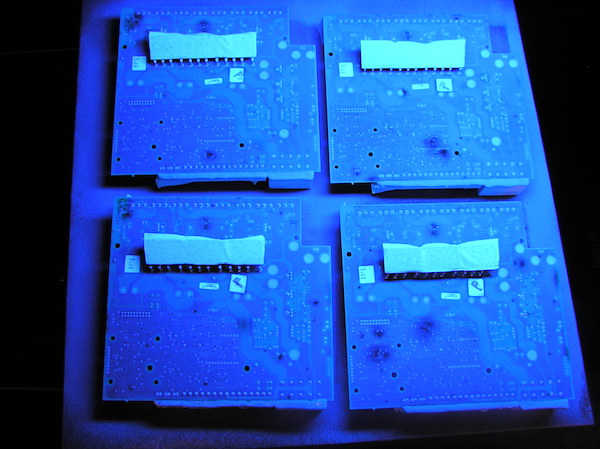
Cleaning the residues left behind by a no-clean flux process is one of the most difficult and misunderstood stages of PCB preparation. These residues are specifically designed to remain on the board, so they are not formulated to be removed easily.

That becomes important when conformal coating is planned. Surface contamination, partially removed residues and poorly matched cleaning chemistry can all affect wetting, adhesion and long-term reliability. The goal is not simply to make the board look cleaner. The goal is to avoid creating a worse failure mechanism than the original residue itself.

Cleaning PCB residues before conformal coating

How do you clean no-clean flux residues if you need to?

Whether a no-clean flux residue can be cleaned effectively depends on the cleaning chemistry’s saponification factor and its compatibility with the residue chemistry present on the assembly.

Saponification is the ability of the cleaning chemistry to soften and break down the residue so it can be dissolved and removed. In simple terms, the more effectively the chemistry attacks the residue, the easier it becomes to clean the surface properly.

The key requirement is complete removal. If the cleaning chemistry does not fully dissolve and remove the residue, the process may create more risk rather than less.

Reality check: A partially cleaned no-clean residue may be more dangerous than a residue left untouched, because the protective resin matrix can be disturbed without fully removing the active chemistry beneath it.

What happens if the residues are only partially dissolved?

A no-clean residue that is only partly cleaned away may be far worse for a printed circuit board assembly than a no-clean residue left untouched. One reason is that lead-free flux activators are generally more active than those used in earlier leaded formulations.

When the residue is left in place, the activators are held within the carrier resin matrix. At normal operating temperatures, that matrix helps keep the residue stable and reduces the risk of corrosion-related problems.

However, if the protective matrix is only partly removed by an inadequate cleaning process, the active chemistry may become exposed. This can initiate corrosion on the circuit board and may be accelerated by heat, electrical bias in service or high relative humidity.

Why this matters for conformal coating

Conformal coating is often applied to improve environmental protection and long-term reliability. But coating over contamination or marginally cleaned residues can lock defects into the assembly rather than eliminate them.

If cleaning is incomplete, the result may include poor coating wetting, reduced adhesion, localised dewetting, corrosion risk and reliability problems that only appear later in service.

This is why cleaning should be treated as a controlled process step, not as a cosmetic operation. If you are reviewing coating failures, it is also worth understanding how poor preparation interacts with broader process issues covered in our article on why conformal coating fails in complex PCB assemblies.

So how should no-clean residues be assessed?

When considering whether to clean no-clean residues before coating, three questions matter:

  1. Can the residue actually be cleaned effectively on this assembly?
  2. Have you matched the cleaning chemistry to the degree of difficulty and the available cleaning process?
  3. Have you validated the overall process by testing, rather than assumption?

These questions matter because no-clean fluxes vary, assemblies vary and cleaning processes vary. A workable answer on one product may fail on another. Validation is essential.

Why Choose SCH Services?

SCH Services supports conformal coating users with practical process knowledge, coating services, training and engineering support. If you are reviewing cleaning, coating adhesion or broader process reliability, we can help assess the issue in the context of the full coating process rather than as an isolated symptom.

To discuss cleaning, coating preparation or process troubleshooting, contact us or call (+44) 1226 249019.

↑ Back to top

This article is provided as general technical guidance only. Cleaning chemistry, residue behaviour and conformal coating performance vary by assembly, flux system and process conditions. Final process decisions should be validated through suitable trials, inspection and reliability testing.

FAQs Atomic Layer Deposition (ALD)


Atomic Layer Deposition (ALD) is an advanced thin-film coating technology used where extreme thickness control, conformality, and film integrity are required at the nanometre scale. It is increasingly specified for high-reliability electronics, semiconductor devices, optics, energy systems, and biomedical components where conventional coating methods reach their technical limits.

Unlike liquid-applied coatings or conventional vapour deposition processes, ALD builds coatings one atomic layer at a time through a self-limiting surface reaction. This allows engineers to precisely define film thickness, composition, and uniformityβ€”even on complex 3D structures, high-aspect-ratio features, and densely packed devices.

The Atomic Layer Deposition FAQs below provide a practical overview of:

  • What ALD is and how it differs from other CVD-based coating processes
  • The types of materials that can be deposited using ALD
  • How the ALD process works in practice
  • Where ALD is typically used across different industries
  • The key advantages and limitations of ALD compared with alternative coating technologies

This section is intended to give engineers, designers, and procurement teams a clear understanding of when ALD is technically justified and how it fits alongside other advanced coating solutions such as Parylene and liquid conformal coatings.

What is ALD?

Atomic Layer Deposition (ALD) belongs to the family of Chemical Vapour Deposition methods (CVD).

  • It is a deposition process at a nano-scale level within an enclosed vacuum chamber.
  • The deposition process forms ultra-thin films (atomic layers) with extremely reliable film thickness control.
  • This provides for highly conformal and dense films at extremely thin layers (1-100nm).

What coatings are deposited in ALD?

ALD principally deposits metal oxide ceramic films. These films range in composition from the most basic and widely used aluminum oxide (Al2O3) and titanium oxide (TiO2) up to mixed metal oxide multilayered or doped systems.

How does ALD work in practice?

The ALD deposition technique is based upon the sequential use of a gas phase chemical process.

  • Gases are used to grow the films onto the substrate within a vacuum chamber.
  • The majority of ALD reactions use two chemicals called precursors.
  • These precursors react with the surface of a material one at a time in a sequential, self-limiting, manner.
  • Through the repeated exposure to alternating gases there is a build up of a thin coating film.

Where is ALD used?

ALD is used in many different areas including:

  • Micro-electronics
  • Semiconductors
  • Photovoltaics
  • Biotechnology
  • biomedical
  • LEDs
  • Optics
  • Fuel cell systems

What are the Advantages and disadvantages of ALD

Advantages

  • Self-Limiting. The ALD process limits the film thickness. Many other processes like Parylene are dependent upon amount of dimer and will continue to deposit successive polymer layers until it is completely used up.
  • Conformal films. ALD film thickness can be uniform from end to end throughout the chamber. Other coatings like Parylene can have a varied coating thickness across the chamber and the devices being coated.
  • Pinhole free. ALD films can be pinhole-free at a sub-nanometer thickness. Parylene and some other materials are only pinhole-free at micron levels.
  • ALD allows layers or laminates. Most other films including Parylene are single component layers.

Disadvantages

  • High purity substrate. This is very important to the quality of the finish similar to many other vapour deposition processes.
  • ALD Systems can range anywhere from $200,000 to $800,000 based on the quality and efficiency of the instrument. This tends to be 3-4 times the prices of a Parylene system.
  • Reaction time. Traditionally, the process of ALD is very slow and this is known to be its major limitation.
  • Masking challenges. The ALD masking process must be perfect. Any pinhole in the masking process will allow deposition beyond the masking barrier.

What are some of the ALD coatings that can be deposited?

A wide variety of chemistries are possible with Atomic Layer Deposition. They include oxides, nitrides, metals, carbides and sulfides.

Want to know more about Atomic Layer Deposition (ALD) coatings?

Contact us now, call us on +44 (0) 1226 249019 or email your requirements on sales@schservices.com

Hybrid ALD/CVD Coatings for LED Protection – Where Do They Really Fit?


Understanding the role of ultra-thin coatings in LED protection without the hype

Protecting LEDs from long-term exposure to harsh environments is becoming increasingly critical, particularly for outdoor and high-reliability applications. Moisture, salt, UV exposure and thermal cycling all create failure risks that must be managed through coating selection.

There are already multiple established protection strategies including Parylene, liquid conformal coatings, ultra-thin fluoropolymers and encapsulation. Each offers advantages, but all involve trade-offs between protection level, process complexity, optical performance and cost.

Hybrid ALD (Atomic Layer Deposition) / CVD (Chemical Vapour Deposition) coatings are often presented as a new alternative. The key question is not whether they are interesting, but where they realistically fit alongside existing coating technologies.

What is a Hybrid ALD/CVD Coating?

Hybrid coatings combine two thin-film deposition techniques into a layered structure.

  • CVD (used in Parylene) deposits a conformal coating in a vacuum environment
  • ALD deposits extremely thin, controlled layers at atomic scale

In hybrid systems, these layers are applied sequentially to build a multi-layer film. The structure is fundamentally different from traditional coatings, as properties can be engineered layer-by-layer rather than relying on a single material.

The result is an ultra-thin coating system, typically in the nanometre range, with tailored barrier, adhesion and surface properties.

Compare this with traditional coating approaches β†’

Why is this approach relevant for LEDs?

LED protection introduces constraints that are not always present in standard PCB coating.

  • Optical clarity – coatings must not reduce light output
  • UV stability – long-term outdoor exposure
  • Moisture resistance – prevention of corrosion and failure
  • Thermal stability – cycling and elevated temperatures

Hybrid coatings are often positioned as suitable because they are extremely thin, highly transparent and can provide good barrier performance relative to thickness.

In applications where traditional coatings create optical or masking challenges, this type of approach becomes more attractive.

Masking Reduction – Not Elimination

One of the most common claims is that hybrid coatings do not require masking due to their extremely low thickness.

Reality check: Ultra-thin coatings can reduce masking requirements, but they do not remove interface risks completely. Connectors, contact surfaces and critical electrical interfaces still require validation.

Whether masking can be reduced depends on:

  • Connector design and contact force
  • Electrical sensitivity of interfaces
  • Long-term wear and fretting behaviour
  • Customer acceptance criteria

In practice, masking strategy becomes an engineering decision rather than being eliminated entirely.

Performance Compared to Established Coatings

Hybrid coatings are often compared with Parylene and liquid conformal coatings. The comparison is not simply performance-based, but application-dependent.

  • Hybrid coatings – ultra-thin, optically clear, engineered film structure
  • Parylene – proven barrier performance and long-term reliability
  • Liquid coatings – scalable, robust and well understood processes

Hybrid coatings can offer advantages in specific LED applications, particularly where optical performance is critical. However, established coatings still dominate in many applications due to proven reliability and process maturity.

The decision is not which coating is β€œbest”, but which is most appropriate for the application and risk profile.

Process and Cost Considerations

Hybrid ALD/CVD processes are often described as low cost due to reduced masking and simple operation. However, real cost depends on the full system.

  • Equipment investment and process control requirements
  • Throughput and batch size limitations
  • Cycle time and scalability
  • Validation and qualification requirements

While operator interaction may be simple, the overall process must be evaluated at production scale rather than individual step level.

For surface preparation prior to coating, see plasma cleaning for conformal coating, which explains how plasma is used to improve adhesion and surface energy.

Where Hybrid Coatings Actually Fit

From a practical engineering perspective, hybrid ALD/CVD coatings are best positioned as a specialist solution rather than a universal replacement.

  • Suitable for optically sensitive applications such as LEDs
  • Useful where ultra-thin coatings provide a design advantage
  • Complementary to existing coating technologies

For most applications, coating selection remains driven by environment, geometry, process capability and reliability requirements.

In many cases, structured coating strategies using established materials remain the most robust approach.

Final Perspective

Hybrid ALD/CVD coatings represent a technically interesting development, particularly for LED protection where optical and environmental requirements must be balanced.

However, they should be viewed as part of a broader coating strategy rather than a direct replacement for Parylene or conformal coatings.

The key is selecting the right coating approach for the application, not chasing a single β€œbest” material.

Need support selecting the right coating approach?

SCH supports coating selection, process design and validation across conformal coatings, Parylene and hybrid strategies.

Contact us to discuss your application.

↑ Back to top

Note: This article provides general technical guidance only. Final design, safety and compliance decisions must be validated against application requirements and relevant standards.
0
  • Your current order total is £0.00 β€” you must have an order with a minimum of £75.00 to place your order.
0
Your Cart
Your cart is empty
  • Your current order total is £0.00 β€” you must have an order with a minimum of £75.00 to place your order.
Calculate Shipping
  • Your current order total is £0.00 β€” you must have an order with a minimum of £75.00 to place your order.

Conformal Coating UK

Technical banner showing PCB and process icons representing conformal coating, masking, inspection and training on the SCH technical knowledge hub.
Conformal Coating UK
Privacy Overview

This website uses cookies so that we can provide you with the best user experience possible. Cookie information is stored in your browser and performs functions such as recognising you when you return to our website and helping our team to understand which sections of the website you find most interesting and useful.