
Hybrid Coating Strategy: Combining Conformal and Nano Coatings for Complex PCBAs
Solving coating challenges in complex PCB assemblies
Most coating failures in complex PCB assemblies are not caused by the coating itself. They are usually caused by geometry, connector interfaces, contamination risk and process limitations that a single coating process cannot manage reliably.
A hybrid coating strategy addresses this by combining coating technologies into one structured process. Instead of forcing one material to do everything, the process separates function: conformal coating provides primary protection where thickness and insulation matter, while nano coating adds surface enhancement in areas that cannot safely take thick film build.
Hybrid protection is easier to understand once the broader differences between conformal coating, nano coating and Parylene are clear, especially where different regions of the same assembly have conflicting protection requirements.
Related articles: For the upstream problem this solves, see Why Conformal Coating Fails in Complex PCB Assemblies. For realistic edge capability in selective processes, read Selective Conformal Coating Accuracy: Why ±1 mm Is the Reality. For the real strengths and limits of thin fluoropolymer systems, see What Nano Coatings Can and Can’t Do on PCB Assemblies.
1) The problem with single coating approaches
Modern PCB assemblies often include press-fit connectors, tight geometries and mixed functional areas. These create conflicting requirements that a single coating cannot resolve reliably.
- Thick coatings: provide protection but can interfere with connectors
- Thin coatings: may be safer for interfaces but offer limited insulation
- Selective coating: improves placement but does not fully control final flow behaviour
This leads to compromise, inconsistency and increased process risk. Connector behaviour is a major driver of these failures, as discussed in Press-Fit Connectors and Conformal Coating Problems.
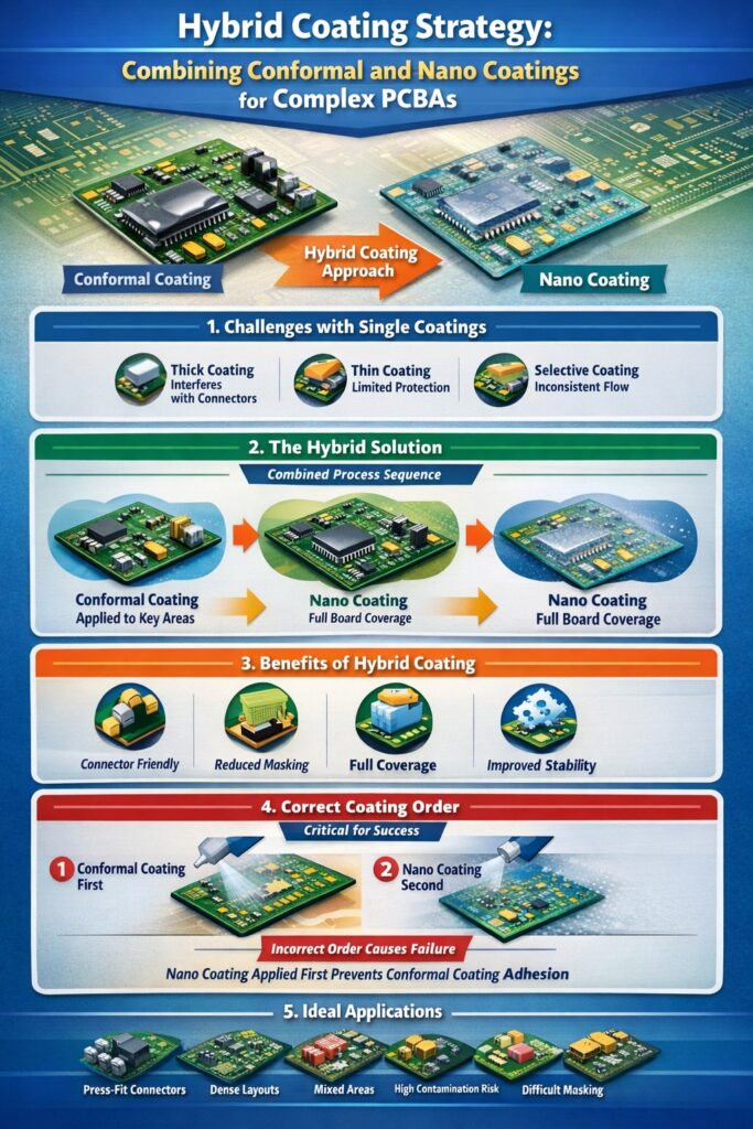
2) Hybrid coating strategy – the structured approach
A hybrid coating strategy combines conformal coating and nano coating into a defined process sequence.
- Apply conformal coating to defined protection areas
- Keep connector-sensitive regions free from thick coating
- Apply nano coating across the entire PCB as a final layer
This creates a system, not just a coating.
This approach is most relevant where a single coating process fails to manage geometry, keep-outs and contamination risk reliably. See Why Conformal Coating Fails in Complex PCB Assemblies.
3) Separation of function – why it works
Each coating is used for what it does best.
- Conformal coating: thickness, insulation and mechanical protection
- Nano coating: full surface coverage, including areas that cannot be coated conventionally
This removes the need to compromise performance or process stability.
This separation only makes sense if the limits of each material are understood clearly. For nano-specific limits, see What Nano Coatings Can and Can’t Do on PCB Assemblies.
Beyond hybrid conformal and nano strategies, some specialist applications are also exploring ultra-thin deposited films where transparency and very low film build are important. For an LED-focused example, see our Insight on hybrid ALD/CVD coatings for LEDs.
4) Managing connectors and critical interfaces
Press-fit connectors are high-risk areas for coating. Capillary action and coating flow can pull material into holes and contact zones, interfering with electrical performance.
The hybrid approach avoids this by structuring protection around function rather than trying to force one material across the whole assembly. These behaviours are driven by coating physics and geometry, not just material choice, as explained in Why Conformal Coating Fails in Complex PCB Assemblies.
- Keeping thick coatings away from contact interfaces
- Using nano coating to provide safe, non-intrusive coverage
- Reducing reliance on complex masking
5) Reducing masking complexity and process risk
Masking is one of the largest sources of variation in coating processes. Complex geometries and tight tolerances make masking difficult to apply consistently.
By allowing nano coating to safely cover sensitive areas, the hybrid model can reduce the burden placed on masking without removing process control where it still matters.
- Masking requirements are reduced
- Operator dependency decreases
- Repeatability improves
Where teams assume selective coating alone will deliver sharp local boundaries, it is worth reviewing Selective Conformal Coating Accuracy: Why ±1 mm Is the Reality.
Important: Nano coatings are not a replacement for conformal coatings. They are an enhancement layer used within a wider system.
6) The role of nano coating in the system
Nano coatings provide:
- Uniform surface coverage
- Hydrophobic behaviour
- Protection in areas that cannot be conventionally coated
They do not provide significant thickness or physical barrier protection on their own. Their limitations need to be understood clearly in system design, as discussed in What Nano Coatings Can and Can’t Do on PCB Assemblies.
Important: Incorrect coating sequence will cause process failure.
7) Coating sequence – critical to success
Correct order:
- Conformal coating first
- Nano coating second
If nano coating is applied first, it creates a hydrophobic surface that prevents proper adhesion of liquid coatings.
8) Where hybrid coating delivers the most value
Hybrid coating is most effective where geometry and function conflict. It is particularly valuable when primary protection is needed in some regions, while other zones must remain free from thick-film interference.
- Press-fit connector assemblies
- Tight track spacing and dense layouts
- Mixed coated and uncoated areas
- Risk of conductive particle contamination
- Applications where masking is difficult or unstable
Where this strategy is applied in practice:
These examples show how coating strategy decisions affect real-world performance, durability and process control.
9) The real decision – process architecture
This is not just a material selection problem. It is a process design decision.
The real engineering question is how to combine boundary control, connector safety, contamination resistance and manufacturability into one stable process.
The key choices are:
- Allow coating everywhere
- Exclude coating from critical areas
- Combine both approaches
The hybrid strategy often provides the best balance between performance, manufacturability and risk.
10) Summary – hybrid coating as a system solution
A hybrid coating strategy delivers a structured solution for complex PCB assemblies.
- Strong primary protection from conformal coating
- Safe full coverage from nano coating
- Reduced masking complexity
- Improved process stability
For complex geometries, combining coatings is often more effective than trying to optimise a single material.
Related process articles
Why Choose SCH Services?
Partnering with SCH means gaining a complete, integrated platform for Parylene and conformal coating—services, equipment, materials and training—built around process control and repeatability.
- ✈️ 25+ Years – trusted worldwide
- 🛠️ End-to-End Support – coating, masking, validation and inspection
- 📈 Scalable Solutions – prototypes to steady production
- 🌍 Global Reach – support across Europe, North America and Asia
- ✅ Process Control – traceability, coupons and inspection discipline
📞 Call: +44 (0)1226 249019 | ✉ Email: sales@schservices.com | 💬 Contact Us ›
Fast links: Parylene Coating Services | Parylene Training & Support | Parylene Equipment
Note: This article provides general technical guidance only. Final design, safety and compliance decisions must be verified by the product manufacturer and validated against applicable standards.
