
Parylene PCB Layout Guidelines
Design rules for component placement, spacing and vapour access
← Back to the Parylene Design Hub
Parylene PCB layout guidelines define how components, spacing and geometry influence coating coverage, masking complexity and long-term reliability. Although Parylene is deposited from the vapour phase and is highly conformal, poor PCB layout can still create shadowing, inaccessible regions and inconsistent coating thickness.
This guide explains the most common PCB layout issues seen in Parylene coating and how to design assemblies that support reliable, repeatable and manufacturable Parylene coating.
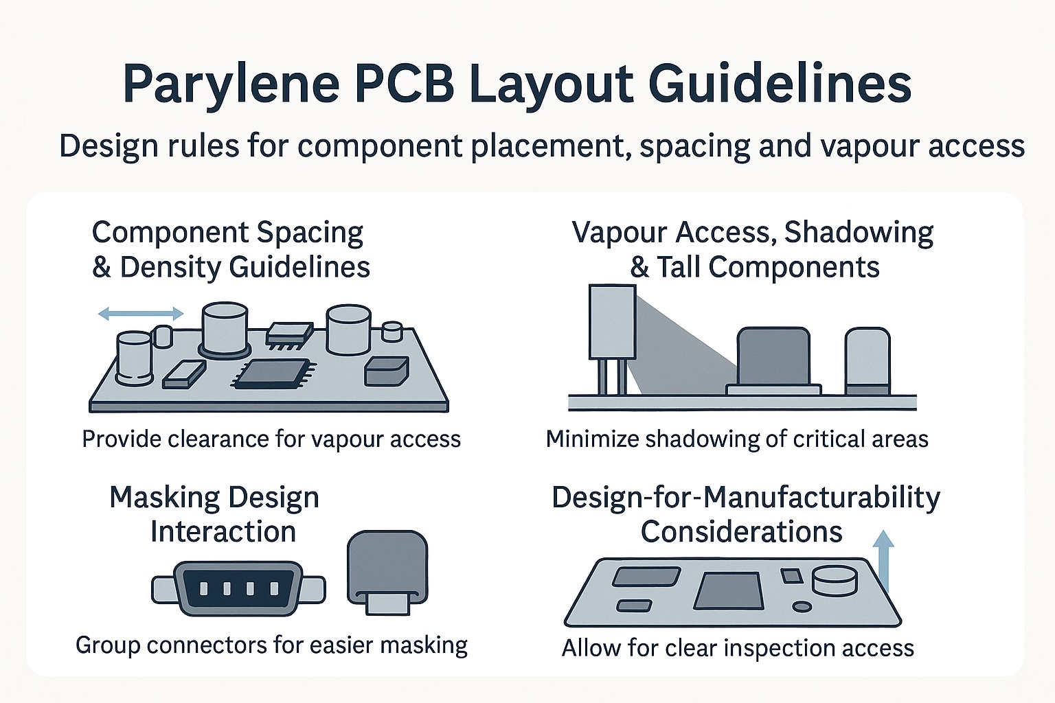
Core PCB layout guidelines that enable reliable, repeatable Parylene coating coverage.
Why PCB Layout Matters for Parylene Coating
Layout guidelines are critical for Parylene because vapour-phase deposition still depends on physical access to surfaces. Layout decisions directly affect:
- Uniformity of Parylene coating under components
- Risk of shadowed or thinly coated areas
- Masking feasibility and cost
- Inspection access and defect detection
Assemblies designed without Parylene PCB layout rules often require rework, additional masking or process compromises.
Component Spacing & Density Guidelines
Good Parylene PCB layout guidelines prioritise spacing that allows vapour access:
- Avoid tightly packed component clusters where possible
- Provide clearance beneath large or low-profile components
- Consider standoff height for BGAs, connectors and shields
Increasing spacing slightly at design stage often reduces coating risk and masking cost later.
Vapour Access, Shadowing & Tall Components
Shadowing occurs when components block line-of-sight vapour flow. Common causes include:
- Tall connectors or housings adjacent to small components
- Vertical walls or dense mechanical features
- Enclosures that limit vapour circulation
Effective Parylene PCB layout guidelines ensure that critical surfaces remain accessible to the vapour stream throughout the deposition cycle.
PCB Layout & Masking Design Interaction
PCB layout and masking design are tightly linked. Layout should:
- Group features that require masking
- Avoid isolated, tiny keep-out areas
- Support the use of standard boots, caps and fixtures
Following Parylene PCB layout guidelines at concept stage reduces masking labour, variability and defect risk.
Design-for-Manufacturability Considerations
Manufacturable PCB layouts for Parylene coating consider:
- Consistent orientation and fixturing
- Handling points that avoid coated surfaces
- Clear inspection access after coating
A layout that coats successfully once may still fail in volume if manufacturability is not considered.
Why Work with SCH on Parylene PCB Layout Design?
SCH supports customers applying Parylene PCB layout guidelines through:
- Design-led reviews focused on spacing, access and manufacturability
- Turnkey capability covering coating services, equipment and materials
- Cross-sector experience in medical, aerospace, automotive and industrial electronics
- Clear scale-up pathways from prototype to production
Call: +44 (0)1226 249019 · Email: sales@schservices.com
Contact SCH to discuss your PCB layout for Parylene coating ›
Disclaimer: This article provides general guidance on Parylene PCB layout guidelines. Performance, suitability and compliance depend on the specific design, materials and application environment. SCH Services can review assemblies and specifications to confirm the most appropriate Parylene coating approach.
