
Parylene Coating for Sensors, MEMS & High-Density Electronics
Ultra-Thin Parylene Protection for Miniaturised, High-Sensitivity Devices
← Back to the Parylene Applications Hub
Parylene coating for sensors, MEMS (Micro-Electro-Mechanical Systems) and high-density electronics is used where devices are small, highly sensitive and exposed to demanding environments. From pressure and inertial sensors to MEMS microphones, biosensors and miniature flex circuits, Parylene offers an ultra-thin, pinhole-free barrier that protects without compromising signal integrity or mechanical response.
Deposited as a vapour-phase polymer film, Parylene uniformly coats complex 3D geometries, microstructures and tight gaps that are difficult or impossible to protect with liquid coatings. Correctly specified, it can improve moisture resistance, corrosion protection, dielectric performance and long-term stability for advanced sensing and microelectronic platforms.
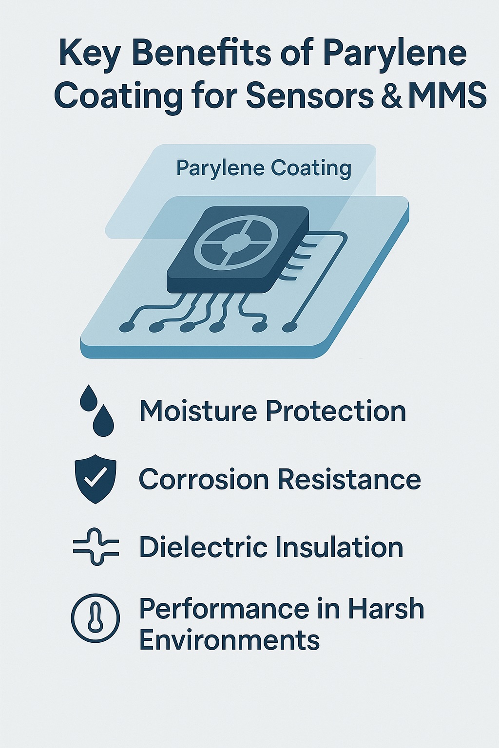
Key benefits of Parylene coating for sensors and MEMS, including ultra-thin conformal protection, dielectric insulation, corrosion resistance and long-term reliability for high-density electronics.
Why Parylene Coating for Sensors & MEMS is Used
Sensors and MEMS devices often operate in environments where moisture, contaminants, condensation or chemical exposure can degrade performance or cause failure. At the same time, their small size and delicate structures mean that any protective coating must be extremely thin and uniform.
A well-engineered Parylene coating for sensors and MEMS offers a combination of properties that is difficult to match with traditional conformal coatings:
- Ultra-thin, low-mass films – typical thickness ranges from 2–15 µm, adding minimal mass and volume.
- Highly conformal coverage – uniform coating on sharp edges, microstructures, cavities and fine interconnects.
- Excellent moisture and vapour barrier – helps protect sensitive elements and interconnects from humidity and condensation.
- Good dielectric performance – high dielectric strength with relatively low dielectric constant for signal integrity.
- Chemical resistance – improved robustness against many process chemicals and environmental contaminants.
- Low-stress deposition – room-temperature vapour deposition without liquid meniscus forces on delicate structures.
When devices must remain stable, repeatable and low-drift over time, a correctly specified Parylene system is often one of the most effective ways to combine environmental protection with tight performance requirements.
Typical Sensor, MEMS & High-Density Applications for Parylene Coating
Parylene coating for sensors and MEMS is used across sectors such as automotive, medical, industrial, consumer and aerospace electronics. Typical examples include:
MEMS & Solid-State Sensors
- Pressure, flow and level sensors in automotive, industrial and process control systems.
- Inertial sensors such as accelerometers, gyroscopes and IMUs.
- MEMS microphones and acoustic transducers in harsh or high-humidity environments.
- Magnetic, position and proximity sensors embedded in confined or sealed assemblies.
Biosensors & Medical Diagnostics
- Implantable and wearable biosensors where biocompatibility and stability are important.
- Lab-on-chip, microfluidic and diagnostic cartridges requiring thin, chemically resistant barrier layers.
- Electrode arrays and microelectrode structures used in monitoring and stimulation applications.
High-Density & Miniaturised Electronics
- Fine-pitch flex circuits and rigid-flex assemblies with limited clearance for conventional coatings.
- High-density interconnects (HDI) and stacked assemblies where 3D coverage is critical.
- Miniature sensor modules integrated into automotive, aerospace and industrial platforms.
In these applications, Parylene is often the primary environmental barrier for tiny mechanical structures, sensing surfaces and interconnects that cannot tolerate thick or uneven liquid coatings.
Design & Engineering Considerations for Sensors & MEMS
To get the best performance from a Parylene coating for sensors and MEMS, devices should be designed and prepared with Parylene in mind from the outset. Key engineering considerations include:
Substrate & Material Compatibility
- Metals, ceramics, silicon and many polymers can be coated successfully when surfaces are clean and stable.
- Low-surface-energy polymers or very smooth surfaces may require surface activation or adhesion promotion.
- Outgassing materials and voids can create bubbles or pinholes and may require pre-bake or alternative design approaches.
Impact on Sensor Response
- Define acceptable changes to sensitivity, damping, frequency response or offset due to added film mass and stiffness.
- Use application trials to determine the minimum viable thickness that still meets barrier and dielectric requirements.
- For exposed sensing surfaces, consider partial coating, patterning or masking strategies to balance protection and response.
Masking & Keep-Out Areas
- Identify keep-out regions (bond pads, connectors, optical windows, acoustic ports, reference openings) early in the design.
- Use appropriate masking tapes, boots, plugs, fixtures or custom tooling to protect these areas during deposition.
- Design mechanical features to reduce shadowing and ensure vapour access where coverage is required.
Thickness Specification
- Typical thicknesses for sensors and MEMS are in the 2–10 µm range, with higher values reserved for very harsh environments.
- Avoid over-specifying thickness, which can add unnecessary mass and mechanical stress or alter device response.
- Use test coupons and representative assemblies to verify that specified ranges are achievable and stable in production.
Selecting the Right Parylene Type for Sensors & MEMS
Different Parylene types offer subtle but important differences in dielectric properties, barrier performance and thermal behaviour. For sensors and MEMS, the most commonly used grades are:
- Parylene C – excellent moisture and chemical barrier with good dielectric strength; widely used for harsh-environment sensors and high-reliability modules.
- Parylene N – very good dielectric properties and flexibility, often chosen for thin coatings where low dielectric constant and signal performance are critical.
- Parylene HT (fluorinated / AF-4 type) – improved high-temperature stability and better resistance to certain chemicals and UV exposure.
The optimum choice depends on factors such as operating environment, temperature range, media exposure, signal characteristics and lifetime requirements. In some cases, evaluation of two candidate Parylene types at different thicknesses provides the best design data for informed selection.
Environmental, Cleaning & Long-Term Stability
Sensors and MEMS devices may be exposed to temperature cycling, humidity, condensation, vibration,
chemicals and contaminants throughout their life. A suitable Parylene coating can help:
- Reduce drift or failure due to moisture ingress or ionic contamination of interconnects.
- Increase robustness against cleaning and wash processes during assembly or maintenance.
- Support thermal cycling and vibration when thickness and adhesion are specified correctly.
- Maintain dielectric and barrier performance over extended field operation.
However, device-level testing remains essential. Parylene should be validated as part of the complete sensor or MEMS design, media exposure and reliability test plan, rather than assumed to solve all environmental issues on its own.
How SCH Supports Sensors, MEMS & High-Density Electronics
SCH Services provides Parylene coating services, equipment, dimers and training for customers working with sensors, MEMS and high-density assemblies. Support can begin at feasibility and extend through to mature volume production:
- Feasibility trials on representative sensor and MEMS hardware to assess coating impact.
- Design-for-Parylene guidance on masking, thickness, materials and fixture design.
- Subcontract Parylene services for prototypes, validation builds and long-term production.
- Turnkey Parylene systems from lab-scale to high-volume equipment, with appropriate process support.
- Operator training and knowledge transfer so in-house teams can run stable, auditable processes.
Call: +44 (0)1226 249019 ·
Email: sales@schservices.com ·
Contact SCH to discuss your sensor or MEMS application ›
🔧 Related Parylene Resources
- Parylene Coating Services
- Parylene Deposition Equipment
- Parylene Dimer Supply
- Design for Parylene – Masking & DfC Guidelines
🔗 Explore More Parylene Applications
- Parylene Coating for Medical Devices & Health Technologies
- Parylene Coating for PCB Protection
- Parylene Coating for Aerospace & Defence Electronics
- Parylene Coating for Automotive & EV Electronics
- Parylene Coating for Sensors, MEMS & High-Density Electronics
- Parylene Coating for Harsh Environments
🌐 External Technical Reference
- IEEE Resources on Sensors & MEMS Design – external reference for sensor, MEMS and microelectronics design considerations, performance and reliability.
Disclaimer: This article provides general guidance only. Performance, suitability and compliance
depend on the specific device design, materials, environment and test requirements. SCH Services can review
assemblies, specifications and test plans to help define an appropriate Parylene coating approach.
