Conformal Coating for High-Frequency RF PCBs — Practical Guidance
How coating thickness, dielectric loading and masking strategy affect RF-sensitive PCB performance
Conformal coating for high frequency RF PCBs is more nuanced than coating typical digital electronics. On many RF layouts, the “space above the trace” is part of the electromagnetic structure — meaning conformal coating is not just environmental protection, it can also influence impedance, insertion loss, antenna tuning and unit-to-unit variation if the coating strategy is not controlled.
This page provides practical, engineering-led guidance. Where performance is sensitive or the environment is harsh, SCH can support with a short technical review so recommendations are accurate and defensible rather than guesswork.

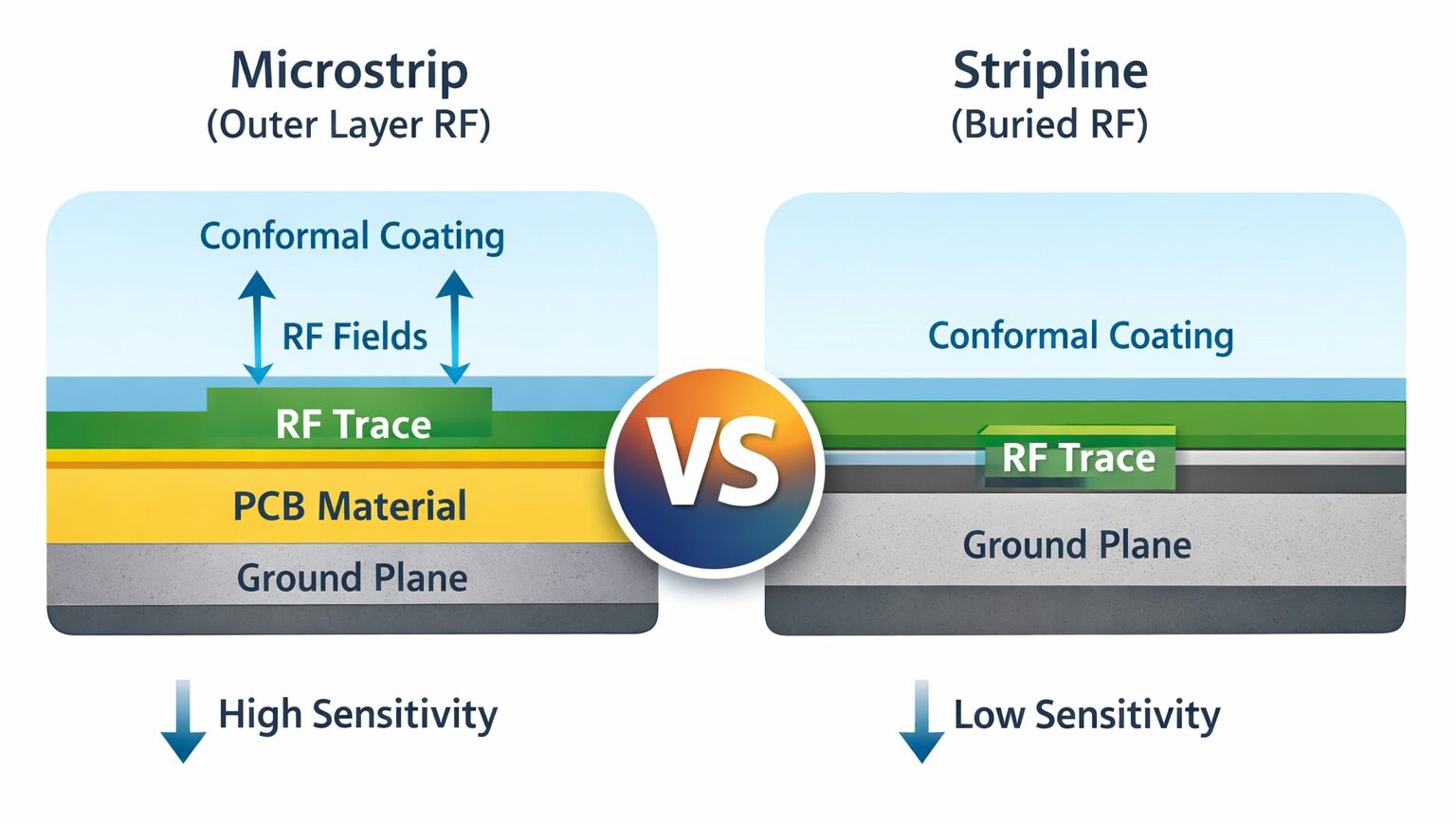
Microstrip routing is typically more sensitive to conformal coating than stripline routing due to exposed RF fields.
Related Knowledge Hubs:
The key idea: conformal coating becomes part of the RF circuit
Many RF transmission lines rely on a predictable dielectric environment. When you apply conformal coating, you replace some of the “air region” with a polymer dielectric. Depending on frequency, geometry and thickness control, this can:
- Shift controlled impedance (enough to matter on sensitive designs)
- Change return loss and insertion loss in critical paths
- Detune resonant structures (filters, matching networks, antennas)
- Increase unit-to-unit variability if thickness is inconsistent
Takeaway: the correct approach depends on where the RF fields actually live — not just coating chemistry.
Microstrip vs stripline: very different coating sensitivity
Microstrip (outer-layer RF) — typically higher sensitivity
Microstrip runs on an outer layer with a reference plane beneath. A significant portion of the electromagnetic field exists above the trace. Adding a conformal coating can meaningfully change the effective dielectric environment, particularly around impedance-controlled sections, transitions, and antenna structures.
Stripline (buried RF) — typically lower sensitivity
Stripline is buried between reference planes. Most of the field is contained within the PCB laminate, so surface coating generally has much less influence on RF behaviour (though antennas, connectors and transitions can still be sensitive).
Practical question to ask early: Are the RF features microstrip, stripline, or coplanar waveguide (CPW)?
Solder mask vs coating: the “hidden” dielectric most people forget
In many designs, the RF area is already influenced by solder mask (or other surface finishes). If a trace is solder-mask covered, adding a thin conformal coating can be a smaller incremental change than many engineers expect. Conversely, exposed-copper RF regions can be more sensitive to any added dielectric layer.
Thickness control often matters more than chemistry
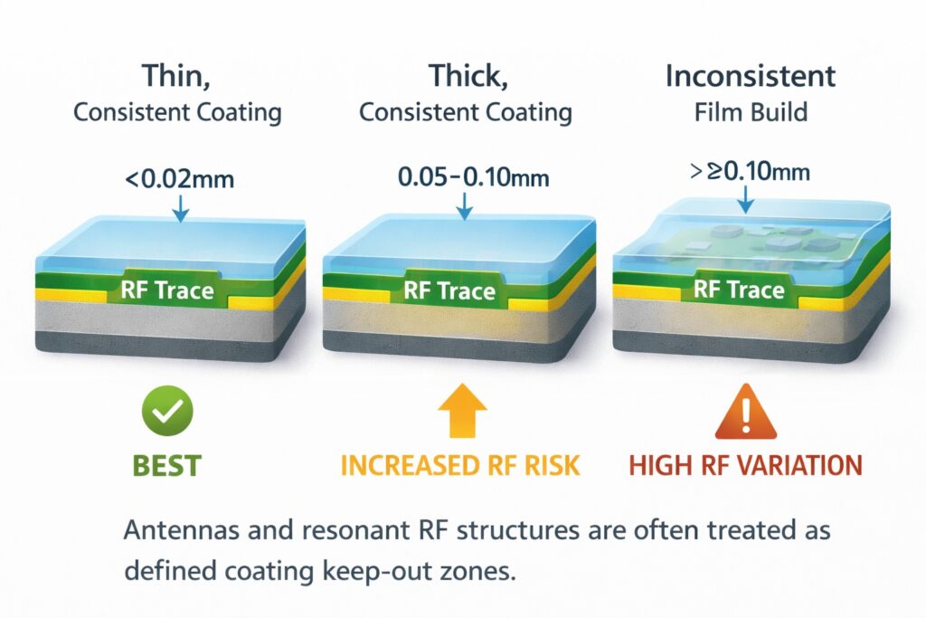
For RF performance, consistency is often as important as material choice. A coating that varies in thickness — or forms local build-ups — can introduce impedance variation and unpredictable behaviour across units.
The difference between a thin, uniform film and a heavy or inconsistent build can materially affect repeatability:

Thin, controlled coatings reduce RF variability compared to heavy or inconsistent film build.
- Thinner, controlled films typically reduce RF risk
- Local build-ups around edges, component bodies and tight gaps can matter more than the “average” thickness
- Keep-out boundaries should be crisp and repeatable (masking quality is critical)
If RF performance sensitivity is high, Parylene is often considered because it can provide very uniform, ultra-thin coverage with controlled thickness across complex geometries.
Where environmental exposure is also a concern, thickness selection must balance dielectric impact and durability margin. See Parylene Thickness & Environmental Protection guidance.
Background reading:
Antennas and resonant RF features: treat as special zones
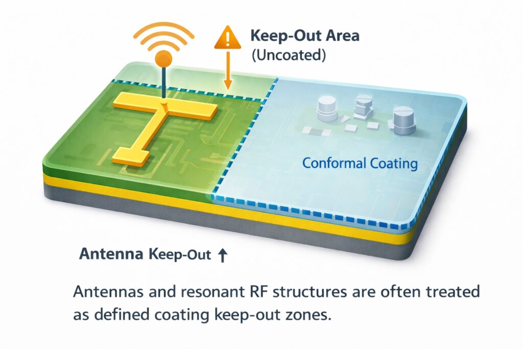
Antennas (printed, chip, patch, edge, etc.) and resonant structures are commonly the most sensitive to dielectric loading. Many robust production strategies use one of the following approaches:
- Keep-out area: leave antenna regions uncoated
- Controlled thin coating: only if testing confirms acceptable detuning
- Defined boundary: a repeatable, well-masked transition between coated and uncoated regions
Rule of thumb: if it radiates, resonates, or sets your RF response, it deserves explicit attention in the coating plan.

Antennas and resonant RF structures are often treated as defined coating keep-out zones.
Moisture and contamination can be worse than coating
In real environments, RF behaviour can drift due to humidity, condensation, ionic residues and contamination. In harsh or outdoor use cases, a thin, stable coating can improve long-term stability and reliability — even if it slightly changes “day-one” RF performance. The correct decision is typically a trade-off between maximum RF performance and environmental robustness.
Practical checklist for RF PCB coating decisions
- What frequency range are we operating in?
- Are critical RF paths microstrip, stripline, or CPW?
- Are RF traces covered by solder mask or exposed?
- Are there antennas or resonant features that need a defined keep-out?
- What environment will the product see (humidity, condensation, salt, vibration)?
- Is thickness tightly controlled and repeatable?
- Is masking strategy defined and validated?
Masking and keep-out control
When RF keep-outs are required, repeatable masking becomes a core part of the process. Poor masking can cause feathered edges, wicking, or leakage into sensitive regions.
Further reading:
How SCH can help
We’re happy to provide general background for free, but for application-specific guidance we normally run a short technical review so we can give you accurate, defensible recommendations rather than guess.
To start, we typically request:
- Frequency range and key RF functions (filters, LNAs, PAs, antennas, etc.)
- Stack-up and RF topology (microstrip / stripline / CPW)
- Any known “do not coat” or performance-critical zones
- Operating environment and reliability goals
If you’re working in compact outdoor or RF-sensitive telecoms/IoT hardware, you may also find this relevant:
External reference
- Overview of conformal coatings, materials and applications: Conformal coating (Wikipedia)
Related reading
Why Choose SCH Services?
RF-sensitive assemblies need a coating strategy that protects the product without introducing avoidable electrical variability. SCH Services helps customers review RF topology, keep-out planning, thickness control and masking practicality so environmental protection is balanced against real performance risk.
- 📡 RF-Aware Coating Guidance – Practical support for microstrip, stripline, resonant structures and antenna keep-out planning.
- 🛠️ Thickness & Process Control – Guidance on uniform film build, masking boundaries and coating repeatability on sensitive assemblies.
- 🔍 Design-for-Coating Input – Help defining realistic do-not-coat zones and production-friendly masking strategies before boards reach manufacture.
- 🌍 Integrated Technical Support – Consultancy, coating services, training and process troubleshooting through one specialist team.
- ✅ Built for Harsh Environments – Support for electronics that must balance RF performance with moisture, contamination and field reliability demands.
📞 Call: +44 (0)1226 249019 | ✉ Email: sales@schservices.com | 💬 Contact Us ›

