Mon - Thur 7.30-15.30   Fri 7.30-14.00

How to Repair Lifted Conformal Coating Edges (Without Making It Worse)


Controlled rework methods using solvent and low-lint swabs to restore clean coating boundaries

Lifted or damaged coating edges are a common issue during conformal coating processes, particularly after masking removal. While often blamed on operator technique, the reality is that coating adhesion, film thickness, cure state, and dwell time all play a significant role in how stable the coating edge remains.

When coating edges lift, tear, or feather, the instinct is often to β€œclean it up” quickly. In practice, this is where additional defects are introduced β€” spreading contamination, damaging adjacent coating, or making the repair more visible than the original issue.

This guide explains how to repair lifted conformal coating edges in a controlled way, without introducing further defects or compromising long-term reliability.

For upstream causes of masking damage and how to prevent it during application, see Masking Application Best Practices.

Low lint swabs for conformal coating rework showing contamination control, precise solvent application and defect prevention

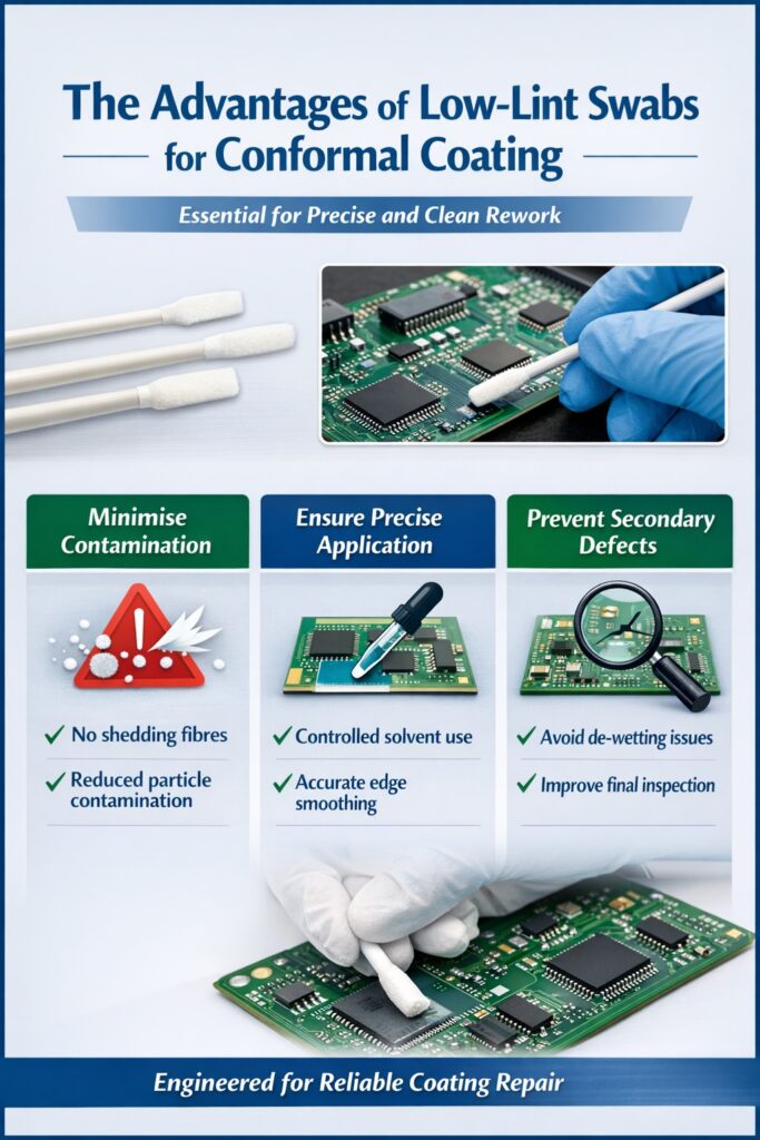
Low-lint swabs enable controlled conformal coating repair by reducing fibre contamination, improving edge definition, and preventing secondary defects during rework.

Why Coating Edges Lift in the First Place

Understanding the cause is critical before attempting repair. Edge lifting is rarely random β€” it is typically driven by a combination of material behaviour, process conditions, and operator handling.

  • Poor adhesion β€” contamination, poor surface preparation, or incompatible substrates
  • Excessive coating thickness β€” thicker films are more prone to tearing during masking removal
  • Cure condition β€” partially cured coatings behave differently to fully cured films
  • Dwell time β€” long delays between masking and removal increase edge stress
  • Operator technique β€” peel angle, removal speed, and handling can either protect or damage coating edges

In practice, edge damage is usually the result of multiple factors interacting, not a single root cause. Even good operator technique cannot fully compensate for poor adhesion, excessive thickness, or incorrect process timing.

If these factors are not understood, repairs will only treat the symptom β€” not the underlying process issue.

What Not to Do

Most coating damage during repair is caused by uncontrolled methods. Avoid the following:

  • Wiping with cloths or tissues β€” introduces fibres and spreads contamination
  • Aggressive scrubbing β€” damages surrounding coating and enlarges the defect
  • Over-applying solvent β€” spreads dissolved coating beyond the repair area
  • Repeated reworking β€” weakens the coating system and affects appearance

If the repair method is not controlled, the β€œfix” often becomes worse than the original defect.

Reality check: Most visible repair defects are introduced during rework rather than during the original coating process.

Correct Method for Repairing Lifted Coating

Effective repair is about control and minimal disturbance, not removal.

Recommended approach

  • Use a compatible solvent β€” matched to the coating chemistry
  • Apply solvent locally using a low-lint swab β€” this allows controlled application without introducing fibres or spreading contamination
  • Gently reflow or smooth the edge rather than removing large areas
  • Work in one direction to avoid spreading material
  • Allow controlled drying before inspection

Low-lint swabs play a key role in this process, allowing controlled solvent application while reducing the risk of fibre contamination β€” a common source of secondary defects during repair.

Warning: Avoid cotton buds or high-lint swabs during repair. Fibre contamination introduced at this stage can directly affect coating performance and inspection results.

The goal is to restore a clean boundary β€” not to rework the entire coated area.

Why Tool Selection Matters

The tool used during repair has a direct impact on contamination risk, edge control, and final finish quality.

  • Low-lint swabs reduce fibre contamination compared to cloths or paper
  • Consistent tip structure allows controlled solvent application
  • Precision handling enables localised repair without affecting surrounding areas

Poor-quality swabs or improvised materials can introduce fibres, leave residue, or damage coating edges β€” especially on fine-pitch assemblies.

Controlled Rework in Practice

In production environments, coating repair should be treated as a defined process step β€” not an improvised activity.

  • Use approved solvents and materials only
  • Define when repair is acceptable vs reject
  • Train operators on controlled rework techniques
  • Inspect repaired areas under appropriate lighting (white light or UV)

This ensures repairs are repeatable, acceptable to inspection, and do not introduce long-term reliability risks.

Recommended Tools for Precision Repair

For controlled coating repair, tool selection should be intentional. In our own coating and rework operations, we use low-lint polyester swabs designed for precision cleaning and localised coating correction.

Warning: Avoid cotton buds or high-lint swabs. While low cost, they can shed fibres into the coating surface, leading to contamination, de-wetting, and visible defects during inspection.

There is often a trade-off between cost and performance. Cotton buds are inexpensive but introduce risk, while specialist cleanroom swabs can be unnecessarily expensive for general coating rework.

Low-lint polyester swabs provide a practical middle ground β€” controlled performance without excessive cost, making them suitable for everyday conformal coating repair and inspection work.

πŸ‘‰ View polyester swabs for conformal coating rework

↑ Back to top

Support Your Coating Process with the Right Tools

Successful conformal coating repair depends on control β€” not just technique, but the materials and tools used during rework.

  • βœ” Low-lint materials to reduce contamination risk
  • βœ” Consistent tip structure for controlled solvent application
  • βœ” Proven performance in real coating and rework environments

πŸ‘‰ View Polyester Swabs for Coating Repair

Note: This article provides general technical guidance only. Repair methods, solvent compatibility, and acceptance criteria must be validated against your specific coating system, materials, and applicable industry standards.

Why ESD protection fails in data centres


Hidden gaps in packaging, infrastructure, handling and environment often undermine static control

ESD protection in data centres often fails because the strategy is too narrow. Controls may exist at workstations or during maintenance, but static risk is still present across packaging, storage, staging areas, infrastructure and mixed-material handling environments.

The result is a familiar problem: a facility appears protected on paper, yet real-world exposure remains across the wider chain of movement and contact.

Quick take. Data centre ESD protection fails when the programme focuses on isolated control points instead of the full environment. Static risk does not begin at the bench or end with a wrist strap.

Why ESD protection fails data centres infographic showing packaging infrastructure maintenance and handling gaps causing electrostatic risk

ESD protection in data centres often fails when packaging, infrastructure, maintenance zones and handling environments are treated as separate issues instead of one connected system.

Why this matters

Data centres depend on reliable movement, installation, storage and replacement of sensitive electronics. Servers, boards, modules and replacement parts pass through multiple environments before and after live operation. Every one of those environments can affect electrostatic risk.

The problem is that ESD protection is still often framed around obvious control points such as wrist straps, mats or workstations. Those controls may be useful, but they only address part of the problem. Static can still be introduced through packaging, mixed materials, temporary holding areas, maintenance activity and infrastructure surfaces.

This means ESD protection can fail without any single dramatic mistake. It fails quietly, through fragmented assumptions and incomplete boundaries.

The pattern we see again and again

Most failures in data centre ESD strategy do not come from having no controls at all. They come from having controls that are too localised.

  • Operators are grounded, but packaging materials are not reviewed.
  • Workstations are controlled, but staging areas use mixed materials.
  • Maintenance procedures exist, but tools, carts and support surfaces vary.
  • Infrastructure is assumed neutral, even where plastics, coatings and inserts behave differently.
  • Teams focus on compliance checks rather than real movement of electronics through the site.

The outcome is a system with pockets of protection separated by practical gaps.

1. Packaging is treated as outside the ESD boundary

One of the biggest reasons ESD protection fails in data centres is that packaging is treated as a logistics issue rather than a handling issue. Yet cardboard, foam inserts, trays, cartons and temporary storage materials are often the first environment the electronics encounters.

If those materials are ignored, static risk may already have been introduced before the equipment reaches the controlled area.

For a focused look at this issue, see The Most Overlooked ESD Risk in Data Centres: Packaging.

2. Operator controls are mistaken for system protection

Wrist straps, heel straps and grounded benches all have value. The failure happens when these are treated as proof that the whole environment is safe.

In reality, operator controls manage charge on a person. They do not automatically control racks, cabinets, packaging, trays, carts, tools or support surfaces. In a data centre, electronics often move through all of these.

For more on this point, see Wrist Straps Don’t Protect Data Centres.

3. Temporary areas become permanent blind spots

Data centres often include temporary environments that are not treated with the same discipline as formal maintenance benches or production-style workstations. These may include staging rooms, unpacking areas, swap-out zones, short-term shelving or transit holding points.

Because these areas are seen as temporary, they can escape detailed review. But in practice, they are often used repeatedly and play a major role in how hardware is handled.

A control strategy that ignores these spaces leaves part of the real workflow outside the protection boundary.

4. Infrastructure surfaces are assumed to be neutral

Another common weakness is the assumption that racks, shelving, support surfaces and cabinets are simply β€œpart of the room” rather than active parts of the ESD environment. In reality, materials, finishes, inserts and attachments all influence how a space behaves.

This does not mean every surface is a problem. It means infrastructure should be reviewed as part of the full handling chain rather than treated as background.

That is why ESD protection in data centres increasingly needs a wider surface and environment perspective.

Practical warning sign. If your ESD programme is strong at the bench but weak in packaging, staging, storage and infrastructure review, the system is probably more fragmented than it appears.

5. Environmental variation is underestimated

Humidity, flooring, mixed materials, repeated movement and maintenance activity all affect how static risk appears in practice. Even where a formal programme exists, local variation can still create weak points.

This is one reason why static control that looks sufficient in theory may not behave consistently in real use. The environment itself changes how risk is expressed across the site.

A robust strategy needs to account for how the environment behaves, not just how the procedure is written.

A more reliable way to think about data centre ESD protection

A better approach is to view the data centre as one connected handling environment rather than a collection of isolated control points.

  • Map where electronics arrive, pause, move, get unpacked and are serviced.
  • Review packaging and temporary materials, not just permanent infrastructure.
  • Assess staging areas, maintenance zones and short-term storage spaces.
  • Look at how surfaces behave across the wider environment.
  • Combine operator controls with broader infrastructure and handling review.

This shifts ESD protection from narrow compliance to practical reliability.

What this means in practice

If your ESD protection has been built mainly around people, benches and formal workstations, the first step is not necessarily to add more rules. It is to look again at the actual journey the electronics takes through your site.

For a broader commercial overview, see our ESD Protection for Data Centres page.

In many cases, the biggest gains come from identifying where protection ends too early rather than from tightening the controls that already exist.

Why Choose SCH Services?

SCH supports customers with practical ESD strategy thinking across infrastructure, packaging, handling environments and surface behaviour. We help identify where static risk is actually introduced in day-to-day operation, then support a more realistic implementation approach.

This is often where a wider environmental review reveals why apparently good ESD programmes still leave practical gaps.

Back to top

Note: This article provides general technical guidance only. ESD control strategy, implementation and validation must be assessed against the specific environment, materials, equipment and applicable standards.

The Most Overlooked ESD Risk in Data Centres: Packaging


Why static risk often begins before equipment reaches the rack

Packaging is often treated as a logistics detail, not an ESD control point. In reality, cardboard, foams, trays, inserts and temporary handling materials can all influence static risk before equipment is even installed.

This creates a blind spot in many data centre environments: the electronics may enter a controlled space, but only after moving through uncontrolled packaging and staging conditions.

Quick take. If packaging, storage and staging materials are ignored, ESD protection starts too late. In many cases, the risk begins before the rack is ever opened.

Packaging ESD risk in data centres infographic showing cardboard foam trays staging areas and handling environments where static can occur

Packaging materials such as cardboard, foams, trays and staging environments can introduce hidden ESD risk before electronics reach controlled data centre areas.

Why this matters

Many ESD programmes focus heavily on workstations, operators and final handling areas. That makes sense on paper, but it can miss a critical part of the journey: how electronics are stored, shipped, unpacked and staged before use.

Servers, boards, modules and replacement parts frequently arrive in mixed packaging systems that include cardboard cartons, foam inserts, plastic trays, temporary protective films and transport aids. These materials may be practical for logistics, but they are not always neutral from an electrostatic point of view.

If packaging is not considered as part of the wider ESD strategy, static risk may already have been introduced before the equipment reaches the controlled area.

This forms part of a wider pattern where ESD protection is fragmented across environments, as explained in why ESD protection fails in data centres.

The pattern we see again and again

In many environments, packaging is seen as temporary, so it is treated as less important than permanent infrastructure. In practice, temporary materials can be involved in repeated handling and repeated risk.

  • Equipment is received in standard packaging and moved into staging areas.
  • Foams, inserts and trays remain in use during unpacking and temporary storage.
  • Components are transferred between boxes, benches, carts and racks.
  • Packaging is reused or repurposed without reviewing its ESD suitability.
  • Attention stays on the operator while the surrounding materials are ignored.

The result is a chain of small exposures that may never appear in formal process maps, but still affect real-world reliability.

Even where operator controls are in place, they do not address packaging-related risk, which is why wrist straps alone are not sufficient.

Why packaging creates hidden ESD exposure

Packaging sits at the boundary between logistics and electronics handling. That is exactly why it gets missed.

  • Cardboard and foams can contribute to charge generation during movement and contact.
  • Plastic trays and inserts vary widely in their ESD behaviour.
  • Temporary staging areas may not have the same controls as formal workstations.
  • Repeated unpacking, repacking and movement adds more handling events.

Because packaging is often short-lived, teams assume it does not matter. But short-lived materials can still create risk during the exact moments when electronics are most exposed.

Practical warning sign. If your ESD controls begin only when the equipment reaches the bench, rack or maintenance station, your real control boundary may be too late.

A better way to think about packaging

A stronger approach is to treat packaging as part of the handling environment, not just as a shipping material.

  • Review what materials sensitive electronics arrive in.
  • Assess how long those materials remain in contact with the product.
  • Look at where unpacking and staging actually happen.
  • Consider whether higher-risk materials can be reduced, replaced or better controlled.

This does not mean every box becomes an engineering project. It means recognising that packaging is often the first real ESD environment the product experiences.

What this means in practice

If packaging is outside your ESD review, there is a good chance your control strategy starts too late. This is especially relevant in data centres where replacement hardware, spares and service parts move repeatedly through temporary holding and handling areas.

For a broader view of infrastructure, staging and handling risk, see our ESD Protection for Data Centres page. To understand how these issues combine at system level, see Why ESD Protection Fails in Data Centres and Wrist Straps Don’t Protect Data Centres.

In many cases, improving packaging awareness is one of the simplest ways to close practical ESD gaps without overcomplicating the wider programme.

Why Choose SCH Services?

SCH supports customers with practical ESD strategy thinking across packaging, handling environments, infrastructure and surface behaviour. We help teams look beyond formal control points and identify where risk is actually introduced in day-to-day operations.

This is often where seemingly minor packaging decisions have a bigger reliability impact than expected.

Back to top

Note: This insight provides general technical guidance only. Packaging materials, ESD control strategy and final implementation decisions must be assessed against the specific equipment, handling environment and applicable standards.

Wrist Straps Don’t Protect Data Centres


Why operator-only ESD control does not address infrastructure and handling risk

Wrist straps are not a complete ESD solution in data centre environments. They control charge on a person, but they do not control the wider infrastructure, surfaces, packaging or handling routes that electronics move through.

This creates a common gap: teams assume ESD is covered because operators are grounded, while static risk continues to exist across the environment.

Quick take. Wrist straps control people. Data centres require control of surfaces, materials and infrastructure. Without that, ESD protection remains incomplete.

Wrist straps ESD data centres infographic showing packaging, racks and maintenance areas where static risk occurs

Wrist straps control operator charge, but ESD risk in data centres exists across packaging, infrastructure, maintenance areas and handling environments.

Why this matters

ESD control is often approached as a compliance task: ensure operators are grounded, provide mats, and follow procedures. In controlled bench environments, this can be effective. In data centres, it is often insufficient.

Electronics in data centres move through multiple stages β€” unpacking, staging, storage, installation, maintenance and replacement. At each stage, different surfaces and materials are involved, many of which can generate or hold static charge.

If those surfaces are not considered, ESD risk is not removed β€” it is simply moved to a different part of the process.

This is one example of a wider issue. In many cases, ESD protection fails due to multiple gaps across the environment, as explored in why ESD protection fails in data centres.

The pattern we see again and again

In many environments, ESD protection is focused heavily on the operator, with less attention given to the wider handling environment.

  • Wrist straps are used during installation or repair work.
  • Packaging materials such as foam and cardboard are not controlled.
  • Racks, trays and storage systems include mixed materials.
  • Maintenance zones introduce tools, carts and temporary setups.
  • Teams assume compliance equals protection.

The result is a fragmented system where some areas are controlled and others are not, even though electronics pass through all of them.

In addition, risk is often introduced before operator control even begins, particularly through packaging and staging environments, as outlined in packaging-related ESD risk.

Why wrist straps alone fall short

Wrist straps are designed as a point-control measure. They do not provide continuous protection across an environment.

  • They only control charge on the person wearing them.
  • They do not influence packaging, trays or infrastructure surfaces.
  • They rely on consistent human use and correct connection.
  • They do not address static generated before or after operator contact.

In data centre environments, where electronics move between multiple surfaces and locations, this creates unavoidable gaps.

Practical warning sign. If your ESD control relies mainly on operator grounding but does not consider packaging, storage and infrastructure surfaces, your protection is likely incomplete.

A more realistic approach

A stronger ESD strategy for data centres combines operator controls with a wider review of the environment.

  • Identify where electronics are stored, moved and handled.
  • Review materials such as packaging, foams, trays and shelving.
  • Assess maintenance and staging areas for repeated contact risks.
  • Introduce more consistent surface behaviour where appropriate.

This shifts ESD control from isolated compliance to system-level reliability.

What this means in practice

Wrist straps should still be used where appropriate. The issue is not removing them β€” it is recognising their limits.

For a broader view of how ESD risk appears across infrastructure and handling environments, see our ESD Protection for Data Centres page. To understand how these issues combine at system level, see Why ESD Protection Fails in Data Centres and The Most Overlooked ESD Risk in Data Centres: Packaging.

In many cases, improving surface consistency and reducing environmental variation has a greater impact than adding more point controls.

Why Choose SCH Services?

SCH supports customers with practical ESD strategy development across infrastructure, packaging, handling and surface behaviour. We focus on how ESD risk appears in real environments, not just how it is defined in procedures.

This is often where moving beyond operator-only thinking improves real-world reliability.

Back to top

Note: This insight provides general technical guidance only. ESD control strategy, implementation and validation must be assessed against the specific environment, materials and applicable standards.

Measurement Reliability on PCBs: Why Eddy Current Often Fails and What to Do Instead


Measuring coating thickness on PCBs is harder than most people expect

Eddy current thickness measurement often gives unreliable results on PCBs. Ground planes, copper density, component proximity and board construction can distort readings, even when the coating itself is consistent.

This insight highlights a common issue: teams trust the number on the gauge without questioning whether the measurement method is valid for that specific PCB.

Quick take. Eddy current measurement works well on flat, conductive substrates β€” but on complex PCBs it can be misleading. Measurement strategy matters more than the tool itself.

Infographic showing why eddy current thickness measurement on PCBs can be inaccurate due to ground planes, copper density, component proximity and measurement location

Eddy current coating thickness measurements on PCBs can be misleading due to ground planes, copper density, component proximity and measurement location β€” making strategy more important than the tool.

Why this matters

Thickness measurement is often treated as a simple validation step: apply coating, measure thickness, confirm compliance. In reality, this step is frequently one of the weakest points in the entire process.

On PCBs, the structure beneath the coating is highly variable. Ground planes, copper layers, tracks, pads and components all influence how measurement devices respond. As a result, two readings taken a few millimetres apart can differ significantly, even when the coating thickness is consistent.

This creates a dangerous situation where good coating processes appear inconsistent, and operators begin adjusting the process to match incorrect data.

The pattern we see again and again

In many production environments, an eddy current gauge is used across the PCB surface without considering where measurements are being taken. Readings are then averaged or compared directly to specification limits.

  • Measurements taken over ground planes show different values to those over sparse copper areas.
  • Readings near components are distorted by geometry and proximity.
  • Operators see variation and assume the coating process is unstable.
  • Process adjustments are made to correct what is actually a measurement problem.

This leads to unnecessary process changes, inconsistent results and reduced confidence in the coating line.

Why eddy current struggles on PCBs

Eddy current measurement relies on electromagnetic interaction with conductive substrates. On simple, uniform surfaces, this works well. On PCBs, the situation is far more complex.

  • Internal copper planes affect signal response.
  • Track density varies across the board.
  • Component proximity alters probe behaviour.
  • Small measurement areas amplify local variation.

The result is not necessarily incorrect measurement β€” but highly context-dependent measurement that must be interpreted carefully.

Practical warning sign. If thickness readings vary significantly across the same PCB but visual coating quality looks consistent, the issue is often measurement reliability rather than coating variation.

A more reliable way to approach measurement

Instead of relying on random PCB measurements, a more robust approach is to define a measurement strategy.

  • Use consistent measurement locations where possible.
  • Understand how PCB structure affects readings.
  • Use witness coupons to provide repeatable reference values.
  • Combine measurement methods rather than relying on one tool.

This approach separates true process variation from measurement artefacts.

What This Means in Practice

If your thickness readings do not make sense, the first step is not to adjust the coating process. It is to question whether the measurement method is appropriate for that PCB.

For related process control topics, see Conformal Coating Processes Hub, Inspection & Quality Hub, and De-wetting in Conformal Coating.

In many cases, a simple change in measurement strategy resolves what appears to be a coating problem.

Why Choose SCH Services?

SCH supports customers with practical coating process validation, measurement strategy and operator training. If your coating thickness data is inconsistent or difficult to interpret, we can help define a more reliable approach based on your specific assemblies and process.

This is often where better measurement removes unnecessary process changes.

Back to top

Note: This insight provides general technical guidance only. Measurement methods, process control and validation must be verified against the specific PCB design, coating system and applicable standards.

Delamination Despite Cleaning: Why Clean Boards Still Fail to Hold Conformal Coating


Cleaning helps, but it does not guarantee adhesion

Delamination after cleaning is often a surface chemistry problem, not simply a cleaning failure. A PCB can appear clean, pass a basic visual check, and still show widespread coating lift if the surface energy is wrong, residues remain that are incompatible with the coating, or the assembly materials do not present a stable surface for adhesion.

This matters because many teams respond by repeating the same cleaning step, using more solvent, or extending wash time, when the real issue is often compatibility, wetting behaviour or surface condition rather than visible dirt.

Quick take. If conformal coating delaminates despite apparently good cleaning, the correct response is usually to review surface energy, residue type, assembly materials, process history and coating compatibility β€” not just to clean harder.

Infographic explaining why conformal coating delaminates after cleaning due to surface energy, residues, material compatibility and process changes on PCBs

Most conformal coating delamination issues are caused by surface chemistry, residues, material compatibility and process changes β€” not simply poor cleaning.

Why this matters

When coating peels, lifts, or separates from a PCB after cleaning, the first assumption is often that the board was not cleaned properly. That is understandable because contamination is a common source of coating defects. However, this explanation is often too simple.

A board can be visibly clean and still be a poor surface for coating adhesion. Extremely thin residues, low surface energy materials, process changes, handling contamination, incompatible repair materials, or a mismatch between cleaning method and coating chemistry can all leave the surface looking acceptable while remaining technically unstable.

That is why β€œclean” and β€œready for coating” are not always the same thing.

The pattern we see again and again

This type of failure often appears on one specific product or PCB design while other assemblies run through the same coating line without obvious issue. The film may lift across a broad area, recede from the surface, peel at edges, or fail during handling, de-masking or later environmental exposure.

That pattern matters because it usually points to a surface chemistry or compatibility issue linked to the board, the residues, the solder resist, the local materials, or the process history rather than a random contamination event.

  • The board may look clean but still carry residues that interfere with wetting or adhesion.
  • The cleaning method may remove loose contamination without changing the underlying surface energy.
  • Different solder masks, finishes, labels, mould compounds and local repair materials may respond differently to the same cleaning route.
  • The coating may be acceptable in general but still be a poor match for the surface condition on that assembly.

In those situations, repeated cleaning often delays the answer rather than solving the problem.

What is usually happening underneath the failure

There are several common mechanisms behind delamination despite cleaning.

Low surface energy

Some surfaces are difficult to wet and difficult for coatings to anchor to. In practical terms, the coating may bead, recede or sit on the surface instead of spreading and bonding properly.

Residues that survive routine cleaning

Not all residues behave the same way. Some are soluble in one cleaner but not another. Others smear or redistribute. A board can therefore pass through cleaning and still carry enough residue to disrupt adhesion.

Assembly-specific material effects

One board may include solder mask changes, component mould compounds, labels, sealants, repaired areas or process residues that make it behave very differently to another assembly that appears similar.

Coating compatibility issues

A coating may perform well on many products but still struggle on a specific surface condition. This is where process understanding becomes more important than assuming the chemistry will tolerate everything.

Practical warning sign. If the same product repeatedly shows adhesion failure while other boards in the same process look fine, the issue is often the interaction between that assembly and the coating process rather than a general cleaning problem.

A more useful way to think about adhesion problems

A weak coating process does not always fail because the line is dirty. It often fails because the surface is not technically prepared for that specific coating. The better engineering question is not simply, β€œWas it cleaned?” but, β€œWas the surface actually suitable for reliable adhesion?”

That means reviewing the full surface condition, including the residue type, the material set on the board, the handling route, the cleaning chemistry, the drying process and the coating selected.

This shift in thinking is often what stops teams from running in circles.

What to review before changing the whole process

Before changing the coating, reworking the line, or blaming the cleaner, it is worth stepping back and checking a few basics.

  • Has the board design, solder mask, flux, cleaning chemistry or handling route changed?
  • Is the failure limited to certain areas, materials or components?
  • Does the coating show poor wetting before cure, or only fail later?
  • Are there local repair materials, labels, sealants or other non-standard surfaces on the board?
  • Is the cleaning method genuinely suitable for the contamination or residue type present?

These questions often reveal that the problem is not random and not simply caused by insufficient wash time.

What This Means in Practice

If coating delaminates despite apparently good cleaning, the next step is not automatically to increase cleaning intensity or change coating chemistry. It is to review the surface condition in a structured way and identify whether the issue is residue, low surface energy, material incompatibility or a process change that has altered the board surface.

For related defect mechanisms, see De-wetting in Conformal Coating, Corrosion and Ionic Contamination, and Why Masking Causes Most Conformal Coating Defects.

For broader inspection and process review context, see the Conformal Coating Inspection & Quality Hub and the Conformal Coating Processes Hub.

This is also where many teams benefit from operator training, structured troubleshooting and practical process review rather than repeated trial-and-error cleaning.

Where this insight fits in the wider coating system

Delamination does not usually sit in isolation. It links directly to masking practice, process sequencing, contamination control, inspection and defect interpretation. That is why this topic is best treated as part of a wider coating reliability system rather than as a standalone cleaning question.

In practical terms, teams often improve faster when they connect adhesion failures to the full process instead of viewing them as one-off surface preparation events.

Why Choose SCH Services?

SCH supports customers with practical conformal coating troubleshooting, training and production-facing engineering support. If your coatings appear to fail despite correct cleaning, we can help review the likely causes and identify a more stable route based on the full process rather than guesswork.

Useful next steps:

This is often where a structured review saves more time than repeating the same cleaning and recoating cycle.

Back to top

Note: This insight provides general technical guidance only. Final design, material selection, surface preparation, process control and validation decisions must be verified by the product manufacturer and confirmed against the applicable standards, qualification requirements and customer specifications.

Why Low-Cost Electronics Still Need High-Performance Coatings


Why even low-cost electronics can require high-performance coating solutions

Low-cost electronics are often deployed in high-risk environments. That creates a contradiction: the product may be inexpensive, but the conditions it operates in demand high-performance protection.

This is where coating decisions become less about unit cost and more about reliability, failure risk and system performance over time.

Quick take. A Β£4 sensor in soil, moisture, chemicals or outdoor environments can still require advanced coating protection. The cost of failure often outweighs the cost of coating.

Visual summary. The diagram below shows why low-cost electronics often require high-performance coating in real-world environments.

Infographic explaining why low-cost electronics still require high-performance coatings due to harsh environments, failure risk and cost of failure

Low-cost electronics are often deployed in harsh environments where failure risk is high, making high-performance coatings essential for reliability despite low unit cost.

The contradiction

Many electronic devices are designed to be low-cost, high-volume products. Sensors, control boards and embedded systems are often built to tight cost targets, sometimes just a few pounds per unit.

At the same time, those same devices may be expected to operate in environments that are far from controlled:

  • soil and moisture exposure
  • condensation and humidity cycling
  • chemicals or fertilisers
  • temperature variation
  • outdoor or industrial environments

This creates a mismatch between product cost and environmental demand.

Why coating becomes critical

Without protection, even a simple electronic assembly can fail quickly in these conditions. Corrosion, leakage paths, contamination and electrical drift can all affect performance.

In these cases, coating is not a premium feature. It is often what allows the product to function reliably at all.

This is where materials such as Parylene can become relevant, even in cost-sensitive applications, because they provide consistent, uniform protection across complex geometries.

Cost vs consequence

The key question is not always β€œhow much does the coating cost?” but β€œwhat does failure cost?”

Failure cost can include:

  • product replacement
  • field service visits
  • loss of data or function
  • customer dissatisfaction
  • brand or reliability impact

In many cases, those costs outweigh the incremental cost of applying a higher-performance coating.

Where it becomes more complex

In some applications, coating does more than protect. It can also influence how the device behaves. This is particularly relevant in sensor systems, where dielectric materials can affect electrical response.

For example, in capacitive sensing applications, coating can change the dielectric environment and shift performance. For more detail, see Why Parylene Coating Changes Capacitive Sensor Performance.

This reinforces the need to treat coating as part of the engineering system, not just a protective layer.

What This Means in Practice

If you are designing or manufacturing low-cost electronics for use in challenging environments, coating should be considered early rather than added as an afterthought.

The goal is not to over-specify protection, but to match the coating approach to the real operating conditions and the cost of failure.

In many cases, this leads to a more balanced decision where coating is treated as part of the product design rather than an optional extra.

Need support selecting the right coating approach?

SCH supports companies in selecting and implementing coating solutions that balance performance, cost and reliability for real-world environments.

This can include material selection, process guidance, coating trials and support for development-stage decisions.

Engineering Consultancy | Parylene Coating Services

Note: This insight provides general technical guidance only. Final design, safety, process control, and compliance decisions must be verified by the product manufacturer and validated against the applicable standards and customer requirements.

Parylene Is Not Always a One-Shot Coating Process


A second layer of Parylene can work β€” but it is not the same as getting it right first time

Parylene is often treated as a one-pass, final coating process, but in practice assemblies are sometimes modified after coating and require further protection. In these cases, a second Parylene layer may be applied over an already coated and locally changed surface.

Our experience shows that this can work in some cases, with the second layer depositing well and restoring useful coverage. However, it should be treated as an engineered recovery option, not a direct equivalent to a single controlled original coating process.

Quick take. Parylene can sometimes be successfully overcoated after rework or modification, but performance depends on the condition of the original coating, the nature of the change and the final application requirements.

Infographic showing second layer Parylene overcoating applied after rework, highlighting coating interface, surface condition, contamination and adhesion considerations

Second-layer Parylene can be applied after rework, but coating interface quality, surface condition and underlying modifications must be carefully assessed.

Why this matters

A common assumption is that once Parylene has been applied, the coating architecture is fixed and cannot be meaningfully altered. In reality, many assemblies go through change after coating, including component replacement, local repair or design updates.

When that happens, the engineering decision is no longer about ideal process flow. It becomes a practical question: can protection be restored without stripping and restarting completely?

That is where second-layer overcoating becomes a useful option to consider.

What we have seen in practice

In recent work, assemblies that had already been coated and then locally modified were overcoated with a second Parylene layer.

The key observation was that the second layer deposited well over the existing surface, providing renewed coverage over the changed areas without obvious visual defects.

This demonstrates that previously coated parts are not automatically excluded from further vapour deposition work when engineering changes are required.

Where the limitation sits

The important point is not whether overcoating is possible. It is how it compares to a first-pass coating on a correctly prepared surface.

A second-layer system introduces additional variables:

  • surface condition and ageing of the original coating
  • handling or contamination prior to recoating
  • local repair materials or modified substrates beneath the new layer
  • interface behaviour between coating layers

Because of this, overcoating should not automatically be treated as equivalent to a single, well-controlled original deposition.

Why overcoating can still work

Parylene is deposited through a vapour-phase process, allowing it to conform to existing surfaces rather than relying on liquid wetting behaviour.

Where the underlying surface is suitable, this allows a second layer to follow the existing geometry and build additional barrier coverage over modified regions.

That is why overcoating can be a credible engineering option, even though it is not identical to a first-pass coating scenario.

Where this is most useful

Second-layer overcoating is most relevant where assemblies have already been coated and then changed, and where a full strip and restart may be disproportionate in cost, time or risk.

  • post-coating engineering changes
  • repair or modification of coated assemblies
  • situations where local protection is no longer sufficient
  • evaluation of recovery options on high-value assemblies

In these cases, overcoating provides a middle ground between local repair and full coating removal.

What This Means in Practice

If a coated assembly has been modified, the next step is not always to strip everything and start again. A second Parylene overcoat may provide a practical way to restore protection.

However, this should be approached as an engineering decision rather than a default process. The condition of the existing coating, the nature of the change and the required performance all need to be considered.

For engineering teams, this creates an additional option β€” not a replacement for getting the original coating process right.

Need support with Parylene rework or overcoating?

SCH supports assessment of rework routes including local repair, strip and recoat, and second-layer overcoating where assemblies have already been modified after coating.

This includes practical evaluation of feasibility, risk and performance based on the specific application rather than assumptions.

Parylene Coating Services | Removal & Rework Systems | Engineering Consultancy

Note: This insight provides general technical guidance only. Overcoating outcomes depend on surface condition, contamination, material compatibility and application requirements. Final decisions should be validated against real assemblies and performance criteria.

Can Parylene Be Removed and Reapplied? Development and Rework Reality


Parylene is not always a one-shot coating process in development

Parylene is often seen as a permanent final coating, but in development work that is not always the full story. In the right circumstances, it can be removed, the device can be modified or re-evaluated, and the product can then be recoated as part of an engineering loop.

This matters because coating is not always the end of the process. In many real projects, it becomes part of testing, tuning, failure analysis and design optimisation.

Quick take. Parylene can be removed and reapplied during development, rework and validation work. That creates a practical workflow of coat, test, strip, modify and recoat, which is often valuable when electrical behaviour, masking, design details or system performance still need to be refined.

Infographic showing Parylene development workflow including coat, test, strip, modify and recoat stages used to optimise coated electronic devices

Parylene development often follows a practical workflow of coat, test, strip, modify and recoat, enabling engineers to optimise performance rather than treat coating as a one-shot process.

Why this matters

A common assumption is that once Parylene has been applied, the part is finished and there is no realistic way back. That assumption can be a problem in development programmes, because many products do not behave exactly as expected on the first coated iteration.

Sensor systems, high-reliability electronics, unusual geometries and electrically sensitive devices can all show behaviour that only becomes visible after coating. In those cases, a development team may need to review the design, make a change, re-test the part and then reapply the coating.

That is where rework capability becomes commercially and technically important. It turns coating from a one-direction process into a development tool.

The practical workflow

In development, the real workflow is often not simply coat and ship. It may be:

  • apply Parylene to a development build
  • test the coated device in real or simulated conditions
  • identify a performance shift, masking issue or design change
  • remove the coating in a controlled way
  • modify, repair or re-evaluate the product
  • recoat and validate again

That loop can be extremely useful in product development because it allows coated performance to be studied rather than guessed.

Why removal and reapplication are valuable

The value is not just that Parylene can be stripped. The value is what that enables.

  • development teams can tune electrical or mechanical performance after seeing real coated behaviour
  • engineering teams can compare coated and recoated results more intelligently
  • failure analysis work can separate coating-related effects from design-related effects
  • prototype programmes do not always have to start from zero after each change

This is particularly relevant where the coating itself influences the operating system, rather than simply protecting it.

A real example of where this matters

In electrically sensitive devices such as capacitive sensors, coating can change the dielectric environment and shift system behaviour. That means development may need more than a single coat-and-test cycle.

Where the coated part shows an unexpected response, a strip and recoat route can support investigation and optimisation rather than forcing teams to treat the first result as final. For related background, see Why Parylene Coating Changes Capacitive Sensor Performance.

That is one reason why removal capability is not just a service feature. It is part of a wider engineering workflow.

Removal is real, but it is not trivial

It is important to be realistic here. Parylene removal is possible, but it is not automatically simple, low-risk or suitable in exactly the same way for every assembly. The method depends on the coating, the substrate, the geometry, the access, the areas to be preserved and the purpose of the rework.

For some projects, localised removal makes sense. For others, a full strip may be required. In some cases, the rework route is best used for development learning rather than routine production reprocessing.

That is why good removal work is engineering-led. It is not just about taking coating off. It is about taking coating off in a controlled way that still leaves the product useful for the next step.

Where this applies beyond development

Although this workflow is most commonly used in development, it is also relevant in repair and rework situations. Localised coating removal is often used to enable component replacement, fault investigation or targeted modification.

In these cases, the goal is usually to restore function rather than optimise performance, and the removal approach is typically more controlled and limited in scope.

Full strip and recoat can be considered, but this is often more complex and must be assessed carefully against time, cost and risk. For many assemblies, particularly complex electronics, a targeted rework approach is more practical.

Why this changes the development conversation

When teams understand that coated parts can be stripped, reviewed and recoated, the discussion shifts. Coating stops being a final irreversible event and becomes something that can support iterative engineering.

That can reduce hesitation around trial builds, help teams learn faster from early results and support a more confident development pathway where coating performance is being actively understood rather than assumed.

For wider technical background on removal methods, trade-offs and engineering considerations, see Ultimate Conformal Coating Removal Guide (UK & Europe) and Identify Unknown Conformal Coatings (IPC-7711).

What This Means in Practice

If your coated device does not behave exactly as expected, the next step is not always to abandon the concept or assume the coating has failed. In many cases, the better route is to treat the coated result as a development input, then decide whether strip, modify and recoat work can move the project forward.

This is where rework capability becomes strategically useful. It supports prototyping, tuning, validation and learning, especially when the coating itself changes system behaviour.

For engineering teams, that makes Parylene more than a protective finish. It makes it part of the development process.

Need support with Parylene development, removal or rework?

SCH supports engineering teams with Parylene coating trials, removal assessment, strip and recoat workflows, and development-stage problem solving where protection and system performance need to be considered together.

This can include development support, controlled rework evaluation, and practical guidance on how to move from an unexpected coated result to a better-defined next iteration.

Parylene Coating Services | Removal & Rework Systems | Engineering Consultancy

Note: This insight provides general technical guidance only. Final design, safety, process control, and compliance decisions must be verified by the product manufacturer and validated against the applicable standards and customer requirements.

Why Parylene Coating Changes Capacitive Sensor Performance


Why Parylene coating can become part of the electrical system in capacitive sensor design

Parylene does not always behave as a passive protective layer. In capacitive sensor systems, it can change the dielectric environment around the sensing structure and shift electrical behaviour in ways that are technically significant.

This insight highlights a real development reality: even with a stable coating process and correct thickness, capacitance and frequency response can still move because the coating becomes part of the working electrical system.

Quick take. In capacitive sensing systems, Parylene can alter field distribution, dielectric behaviour and output response. Thickness matters, but it does not explain performance on its own. Geometry, coverage and system interaction matter just as much.

Infographic showing how Parylene coating changes capacitive sensor performance by altering dielectric environment, electric field distribution and capacitance response

Parylene coating can change the dielectric environment around a capacitive sensor, shifting electric field distribution, capacitance and frequency response even when coating thickness is correct.

What we observed

In a recent project involving a capacitive soil sensor, SCH observed measurable changes in operating frequency and capacitance values after Parylene coating. The coating process itself was stable, thickness was verified using witness coupons, and coverage was consistent.

From a coating process perspective, the job looked correct.

However, the coated sensor did not behave in exactly the same way as the uncoated version. That is the important point. The process was controlled, but the system response still shifted.

Why this happens

Parylene is a high-performance dielectric material. In capacitive systems, dielectric properties are not secondary. They directly influence how the device works.

Once applied, the coating can change the electrical environment by altering the effective dielectric constant around the sensor, changing electric field distribution and modifying how the sensor interacts with the surrounding environment.

In simple terms, the coated sensor is no longer operating in the same electrical condition as the uncoated design.

Why thickness alone does not explain performance

One of the most common assumptions is that coating thickness should explain the result. Thicker coating means larger effect. Thinner coating means smaller effect. That sounds logical, but real systems are rarely that simple.

Thickness matters, but it sits inside a broader interaction that can include sensor geometry, electrode spacing, edge coverage, local coating distribution and the final operating environment.

This is why a coating can be within specification and still produce an unexpected electrical outcome. If you want a broader technical view of how thickness should be considered in protective coating strategy, see Parylene Thickness & Environmental Protection: How Much Is Enough?.

Why geometry and coverage matter

Capacitive fields are not distributed evenly. They concentrate around edges, interfaces, exposed conductors and changes in geometry. Parylene follows those features extremely well, which is normally a major advantage.

In electrically sensitive devices, that same conformality means the coating can influence precisely the areas that matter most to performance. Small changes in how the dielectric layer sits across gaps, corners or sensing boundaries can shift field behaviour enough to affect output.

That is one reason why two coatings that look visually identical can still influence electrical behaviour differently in a highly sensitive design.

What this means in development

For capacitive sensors and other field-dependent electronics, coating should not always be treated as a final passive protection step. It often needs to be treated as a design variable that is considered during validation.

That may mean comparing coated and uncoated versions, reviewing whether the geometry makes the design coating-sensitive, and using strip, modify and recoat cycles during optimisation.

If you are weighing coating choice more broadly at system level, it may also be useful to review Parylene vs Conformal Coating Selection Guide.

What This Means in Practice

If a sensor behaves differently after coating, that does not automatically mean something has gone wrong with the process. In many cases, it means the coating has become part of the working electrical system and must be engineered accordingly.

Where development teams need to test, modify and re-evaluate coated parts, SCH can also support removal and rework workflows. For broader background on engineering-led rework, see Ultimate Conformal Coating Removal Guide (UK & Europe).

This is where coating stops being just a protection layer and becomes part of the engineering design conversation.

Need support with Parylene and electrically sensitive devices?

SCH supports development-stage Parylene projects where environmental protection, electrical behaviour and iterative optimisation all need to be considered together.

This can include coating trials, engineering review, strip and recoat work, and support for sensor and electronics development programmes.

Parylene Coating Services | Removal & Rework Systems | Engineering Consultancy

Note: This insight provides general technical guidance only. Final design, safety, process control, and compliance decisions must be verified by the product manufacturer and validated against the applicable standards and customer requirements.

0
  • Your current order total is £0.00 β€” you must have an order with a minimum of £75.00 to place your order.
0
Your Cart
Your cart is empty
  • Your current order total is £0.00 β€” you must have an order with a minimum of £75.00 to place your order.
Calculate Shipping
  • Your current order total is £0.00 β€” you must have an order with a minimum of £75.00 to place your order.

Conformal Coating UK

Technical banner showing PCB and process icons representing conformal coating, masking, inspection and training on the SCH technical knowledge hub.
Conformal Coating UK
Privacy Overview

This website uses cookies so that we can provide you with the best user experience possible. Cookie information is stored in your browser and performs functions such as recognising you when you return to our website and helping our team to understand which sections of the website you find most interesting and useful.