In modern electronics and high-reliability assemblies, one of the most overlooked yet critical steps is masking—protecting areas that must remain coating-free during the conformal coating process. Done poorly, masking becomes a bottleneck: misalignment, rework, and delays can cripple throughput. But with custom masking shapes for conformal coating, you can turn that bottleneck into a breakthrough.
Explore our range of custom masking shapes for conformal coating designed to speed setup, improve consistency, and boost production yield.
The Masking Challenge
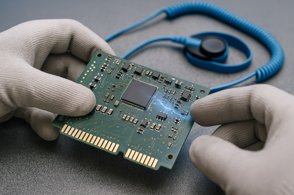
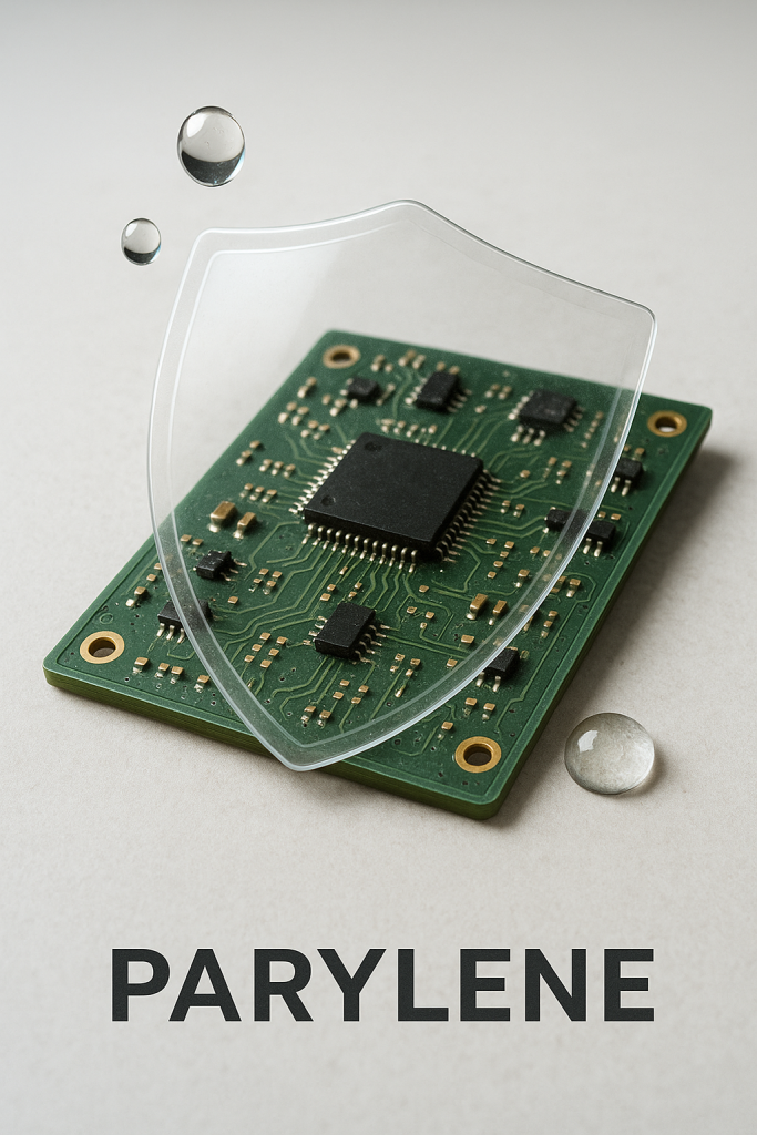
When applying conformal coatings—or advanced materials like Parylene—pads, connectors, keep-out zones, and sensitive features must be protected precisely. Traditional manual cutting of tape is slow, inconsistent, and often unreliable.
The result?
- Masking residue left behind
- Shrinkage or degradation under solvents
- De-wetting caused by silicone contamination
- Tape lifting or coating bleed into protected areas
These issues reduce yield, increase rework, and slow down production.
For a full breakdown of masking options and where each is best used, see Conformal Coating Masking: Methods & Materials.
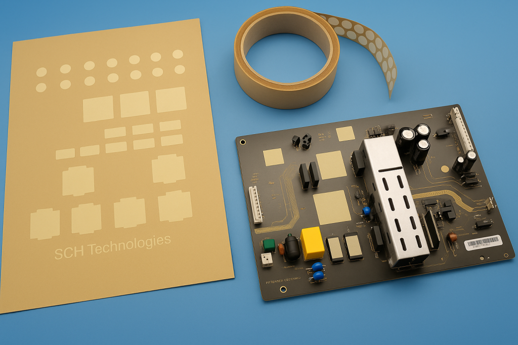
The Advantage of Custom Masking Shapes
At SCH Services Ltd, we provide custom masking shapes designed specifically for conformal coating processes—including the same materials we use in our own production services. That means the shapes we supply are proven daily for accuracy, consistency, and clean removal.
Benefits of custom shapes include:
- Residue-free removal with no damage to components
- Solvent and chemical resistance for demanding environments
- Silicone-free materials to reduce contamination and coating defects
- Clean, reliable adhesion that helps prevent lifting and bleed
- Ready-to-use sheets for fast application and reduced operator time
Because we rely on these shapes daily in our own conformal coating services, we know firsthand how they improve throughput, reduce defects, and remove bottlenecks.
For standard formats or fast turnaround requirements, custom masking dot and shape sheets can also be ordered directly via our online shop. Order custom masking dot and shape sheets online.
From Bottleneck to Breakthrough
Standardising masking with custom masking shapes for conformal coating improves speed and repeatability—while reducing operator variation.
| CHALLENGE | MANUAL MASKING | CUSTOM MASKING SHAPES |
| Cutting & prep time | High | Minimal – peel & place |
| Consistency | Operator dependent | Uniform every time |
| Risk of rework/defects | High | Low |
| Cycle efficiency | Slow | Streamlined |
| Yield loss | Frequent | Reduced |
By reducing cutting time and improving repeatability, masking becomes faster, cleaner, and more reliable—supporting higher yield and smoother production flow.
SCH Services Ltd: Proven in Our Own Services
Unlike suppliers who only sell materials, SCH Services Ltd actively uses these masking shapes in our own conformal and Parylene coating services. Customers benefit from the same speed, precision, and clean demasking performance we demand for our own clients.
When reliability matters, masking isn’t a bottleneck—it’s a breakthrough.
If you’re ready to standardise masking in your production, learn more about custom masking shapes for conformal coating and how they can reduce defects and cycle time.
If you already know your masking requirements, you can order custom masking dot and shape sheets directly from our shop, or contact us for fully bespoke designs.