
Why Parylene coating can become part of the electrical system in capacitive sensor design
Parylene does not always behave as a passive protective layer. In capacitive sensor systems, it can change the dielectric environment around the sensing structure and shift electrical behaviour in ways that are technically significant.
This insight highlights a real development reality: even with a stable coating process and correct thickness, capacitance and frequency response can still move because the coating becomes part of the working electrical system.
Quick take. In capacitive sensing systems, Parylene can alter field distribution, dielectric behaviour and output response. Thickness matters, but it does not explain performance on its own. Geometry, coverage and system interaction matter just as much.
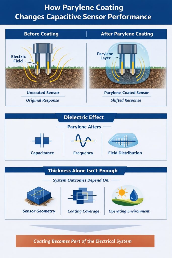
Parylene coating can change the dielectric environment around a capacitive sensor, shifting electric field distribution, capacitance and frequency response even when coating thickness is correct.
What we observed
In a recent project involving a capacitive soil sensor, SCH observed measurable changes in operating frequency and capacitance values after Parylene coating. The coating process itself was stable, thickness was verified using witness coupons, and coverage was consistent.
From a coating process perspective, the job looked correct.
However, the coated sensor did not behave in exactly the same way as the uncoated version. That is the important point. The process was controlled, but the system response still shifted.
Why this happens
Parylene is a high-performance dielectric material. In capacitive systems, dielectric properties are not secondary. They directly influence how the device works.
Once applied, the coating can change the electrical environment by altering the effective dielectric constant around the sensor, changing electric field distribution and modifying how the sensor interacts with the surrounding environment.
In simple terms, the coated sensor is no longer operating in the same electrical condition as the uncoated design.
Why thickness alone does not explain performance
One of the most common assumptions is that coating thickness should explain the result. Thicker coating means larger effect. Thinner coating means smaller effect. That sounds logical, but real systems are rarely that simple.
Thickness matters, but it sits inside a broader interaction that can include sensor geometry, electrode spacing, edge coverage, local coating distribution and the final operating environment.
This is why a coating can be within specification and still produce an unexpected electrical outcome. If you want a broader technical view of how thickness should be considered in protective coating strategy, see Parylene Thickness & Environmental Protection: How Much Is Enough?.
Why geometry and coverage matter
Capacitive fields are not distributed evenly. They concentrate around edges, interfaces, exposed conductors and changes in geometry. Parylene follows those features extremely well, which is normally a major advantage.
In electrically sensitive devices, that same conformality means the coating can influence precisely the areas that matter most to performance. Small changes in how the dielectric layer sits across gaps, corners or sensing boundaries can shift field behaviour enough to affect output.
That is one reason why two coatings that look visually identical can still influence electrical behaviour differently in a highly sensitive design.
What this means in development
For capacitive sensors and other field-dependent electronics, coating should not always be treated as a final passive protection step. It often needs to be treated as a design variable that is considered during validation.
That may mean comparing coated and uncoated versions, reviewing whether the geometry makes the design coating-sensitive, and using strip, modify and recoat cycles during optimisation.
If you are weighing coating choice more broadly at system level, it may also be useful to review Parylene vs Conformal Coating Selection Guide.
What This Means in Practice
If a sensor behaves differently after coating, that does not automatically mean something has gone wrong with the process. In many cases, it means the coating has become part of the working electrical system and must be engineered accordingly.
Where development teams need to test, modify and re-evaluate coated parts, SCH can also support removal and rework workflows. For broader background on engineering-led rework, see Ultimate Conformal Coating Removal Guide (UK & Europe).
This is where coating stops being just a protection layer and becomes part of the engineering design conversation.
Need support with Parylene and electrically sensitive devices?
SCH supports development-stage Parylene projects where environmental protection, electrical behaviour and iterative optimisation all need to be considered together.
This can include coating trials, engineering review, strip and recoat work, and support for sensor and electronics development programmes.
Parylene Coating Services | Removal & Rework Systems | Engineering Consultancy
