Mon - Thur 7.30-15.30   Fri 7.30-14.00

Are there design rules for applying conformal coatings?


Conformal coating is not simply a consumable material. Unfortunately, for too many designers, conformal coating is simply a part number, to be applied to circuit boards. However, this can be a major problem especially in the conformal coating production stage of the process.

There are guidelines in the IPC standards that may help with Design for Manufacture (DFM) principles. These are worth considering. Unfortunately, there are no official design guidelines that will help directly with the application process and conformal coating.
Conformal coating treated as a part number rather than a design consideration can cause production issues

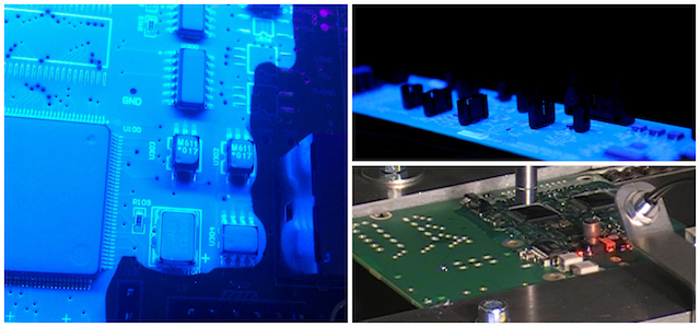
When conformal coating is treated as a simple part number rather than a design consideration, it can create significant problems during the production stage.

Conformal Coating Design Hub

SCH Services Ltd has developed design rules for conformal coating in their Design Hub to help users get the fundamentals right.

The hub focuses on designing PCBs and assemblies for coating, including keep-out zones, component spacing, creepage and clearance, and applying DfM/DfCC principles before manufacture. The philosophy is that for companies embracing lean philosophies and applying conformal coatings, a failure to appreciate the subtleties of the application process can result in an un-coatable (at least as specified) assembly process.

The problem is if the rules are not followed, the resultant circuit board design can challenge even the most sophisticated conformal coating system and its operator to achieve the finish desired.

For further information visit conformal coating design rules to learn more.


Need Process Support?

Optimising electronics coating methods requires the right combination of materials, equipment, and operator training. Partner with SCH Services for:

Infographic explaining whether MIL-SPEC qualification is required for conformal coating and how legacy MIL-I-46058C references relate to modern standards.

Do you need MiL spec qualification for your conformal coating?


A common question from aerospace and defence customers is: β€œDo we need MIL-SPEC qualification for our conformal coating?”

The short answer is: sometimes β€” but only when it is contractually required.

Confusion usually arises because legacy military standards are still referenced on drawings, purchase orders, or coating datasheets, even though the underlying standards landscape has changed.

For a full explanation of how military (MIL) requirements relate to modern conformal coating standards, see: MIL-I-46058C (Cancelled) & MIL Standards for Conformal Coating
.


When is MIL-SPEC actually required?

In practice, manufacturers usually know they require MIL-related compliance when:

  • The product is for a military or defence programme
  • MIL requirements are explicitly called up on the customer drawing
  • The purchase order or contract includes MIL flow-down requirements

If none of these are present, β€œMIL-SPEC” is often being used as shorthand for high reliability rather than a defined manufacturing requirement. This is where misunderstandings commonly occur.


Be cautious with datasheets claiming β€œmeets MIL-I-46058C”

Many conformal coating datasheets state that the material β€œmeets the requirements of MIL-I-46058C”. This wording should be treated with caution.

MIL-I-46058C is a cancelled standard, and simply stating compliance does not mean the coating has been independently approved or qualified. In many cases, the claim refers only to internal or historical test data.

Where defence programmes genuinely require MIL-style material qualification, customers will often expect evidence beyond a datasheet statement.


What is the Qualified Product List (QPL)?

Historically, conformal coatings tested against MIL-I-46058C were listed on the Qualified Product List (QPL).

The MIL-I-46058C Conformal coating standard has been inactive for new designs since the late 1990s, but QPL listings are still referenced in legacy documentation and long-lifecycle programmes.

Coatings appearing on the QPL would have undergone independent third-party testing rather than self-certification. This is an important distinction.

However, the presence (or absence) of a coating on the QPL does not automatically determine its suitability for modern programmes. What matters today is how customer requirements are defined and verified.


What is normally used instead today?

Modern defence and aerospace programmes typically rely on a combination of:

  • IPC-CC-830 for conformal coating material performance and qualification
  • IPC-A-610 for workmanship and acceptance criteria
  • Customer drawings and specifications defining coverage, keep-out zones and inspection evidence

MIL requirements are therefore usually met through industry standards plus contractual flow-downs, rather than through a single active β€œMIL-SPEC” document.


Need to understand how the standards fit together?

The Conformal Coating Standards Hub brings together SCH’s guidance on IPC-A-610, IPC-CC-830, IEC 60664, UL 746, NASA workmanship standards and how they relate to conformal coating and Parylene.

It is designed to help engineering, quality and procurement teams understand:

  • What each standard actually covers
  • How acceptance, material qualification and inspection requirements interact
  • Where legacy MIL references still appear β€” and how to interpret them safely

You can also explore related hubs covering Design, Inspection & Quality and Parylene Coating.


If you need help interpreting customer requirements, legacy MIL references, or selecting compliant coating materials and inspection criteria, contact SCH Services.

πŸ“ž Call: +44 (0)1226 249019 Β | βœ‰ Email: sales@schservices.com

What is Plasma Cleaning?


Plasma cleaning is a process of using plasma energy to clean and modify the surface of a substrate like a circuit board assembly. It is a highly effective surface cleaning and treatment process before application of conformal coatings and Parylene and is gaining more popularity due its highly effective performance.

Plasma cleaning is a process of using plasma energy to clean and modify the surface of a substrate like a circuit board assembly. It is a highly effective surface cleaning and treatment process before application of conformal coatings and Parylene.

What is Plasma?

Plasma is the energy-rich gas state (also known as the fourth state of matter) that can be used to modify the surface of a product to improve its performance.

Plasma technology is based on a simple physical principle. Matter changes its state when energy is supplied to it. Solids become liquid. Liquids become gas. If additional energy is then fed into a gas by means of electrical discharge it eventually ionises and goes into the energy-rich plasma state, plasma is created.

This modification can be improving the adhesion of a conformal coating or change the surface characteristics of the board.


How is Plasma used for improving the performance of coatings with printed circuit boards?

For electronic circuit surfaces, plasma treatment can be used in two highly effective ways.

That is it can:

  • Clean the surface of the circuit board. The surface will be free of residues and 100% contamination free including release agents and additives.
  • Activate the surface of the circuit board assembly. This will allow easier bonding and better adhesion of conformal coatings and Parylene.

These properties make it an interesting technique for improving the surface performance of an electronic circuit board.

In fact, plasma treatment can clean, activate or coat nearly all surfaces. These surfaces include plastics, metals, (e.g., aluminum), glass, recycled materials and composite materials. This means the plasma process can be highly effective on many different products.


How is the plasma applied to a circuit board to clean and activate the surface?

For materials like liquid conformal coatings and Parylene then atmospheric pressure plasma is an excellent process for cleaning surfaces and improving adhesion and surface energy performance of circuit boards.

Atmospheric plasma is generated under normal pressure. This means that low-pressure chambers are not required. The plasma is created with clean and dry compressed air and does not require forming gases. It is possible to integrate plasma directly into manufacturing processes under normal pressure conditions.

Typical plasma components used for cleaning surfaces on circuits are:

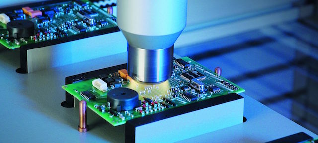
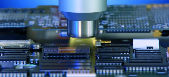
  • Plasma jets (nozzles) to apply the plasma to the surface of the circuit board. They could be controlled by a robotic system.
  • The plasma generators that create the plasma to clean or supply the coatings as required. They provide output power and, in conjunction with complete pretreatment stations, assume various control functions.
  • The process monitoring that controls the nozzles, the movement of the system and the quality of the output.

These three parts form the plasma cleaning process.


Want to know more about plasma cleaning and conformal coating performance?

Contact us now to discuss what we can do to help. Or, give us a call at (+44) 1226 249019 or email your inquiries at sales@schservices.com

How to clean “no clean” flux residues and get it right


Cleaning the residues left behind by a no clean flux process is one of the most difficult tasks when considering cleaning. After all, the residues left on the circuit board are not formulated to be cleaned away easily.

How do you clean “no clean” flux residues if you need to?

Whether a flux residue can be cleaned effectively depends on the cleaning materials saponification factor and its compatibility with the residues.

Saponification is the ability of the no clean residues to be softened to the point of being able to be dissolved by the alkali content (the saponifier) of the cleaning chemistry. The higher the saponification factor of the cleaning fluid the easier it is to clean the residues.

So the key here is to ensure that the saponifier completely dissolves the residues.

What happens if the residues are only partially dissolved?

A no-clean residue that is only partly cleaned away may be far worse for a printed circuit board assembly (PCBA) than a no-clean residue left untouched. One of the reasons is because lead free flux activators are more active than those in earlier leaded flux formulations.

In a no clean flux, when un-cleaned, the residues are locked up in the carrier resin matrix. They are stable (benign) at normal operational temperatures and therefore will not leach out dangerous residues and cause corrosion problems. However, if the protective matrix around the residue is partially removed by an inadequate cleaning regime, then the activators could be exposed.

This may lead to a corrosion process starting on the circuit board. Further, this process could be accelerated in the presence of heat, power on the boards in service or high relative humidity.


So how do you clean β€œno-clean” residues?

It is important when considering cleaning β€œno-clean” residues on a circuit board that you consider three points:

  1. Can you actually clean the residue to be cleaned effectively?
  2. Have you matched the cleaning chemistry with the relative degree of difficulty and the available process?
  3. Have you validated the whole process by careful testing?

Consider these three points and it may help you be successful. Not considering these three points could easily lead you to having real problems in the long term.


Want to know more about cleaning no clean fluxes or cleaning circuit boards?

Contact us now to discuss what we can help you with your cleaning issues. Β Or, give us a call at (+44) 1226 249019 or email your inquiries at sales@schservices.com

FAQs Atomic Layer Deposition (ALD)


Atomic Layer Deposition (ALD) is an advanced thin-film coating technology used where extreme thickness control, conformality, and film integrity are required at the nanometre scale. It is increasingly specified for high-reliability electronics, semiconductor devices, optics, energy systems, and biomedical components where conventional coating methods reach their technical limits.

Unlike liquid-applied coatings or conventional vapour deposition processes, ALD builds coatings one atomic layer at a time through a self-limiting surface reaction. This allows engineers to precisely define film thickness, composition, and uniformityβ€”even on complex 3D structures, high-aspect-ratio features, and densely packed devices.

The Atomic Layer Deposition FAQs below provide a practical overview of:

  • What ALD is and how it differs from other CVD-based coating processes
  • The types of materials that can be deposited using ALD
  • How the ALD process works in practice
  • Where ALD is typically used across different industries
  • The key advantages and limitations of ALD compared with alternative coating technologies

This section is intended to give engineers, designers, and procurement teams a clear understanding of when ALD is technically justified and how it fits alongside other advanced coating solutions such as Parylene and liquid conformal coatings.

What is ALD?

Atomic Layer Deposition (ALD) belongs to the family of Chemical Vapour Deposition methods (CVD).

  • It is a deposition process at a nano-scale level within an enclosed vacuum chamber.
  • The deposition process forms ultra-thin films (atomic layers) with extremely reliable film thickness control.
  • This provides for highly conformal and dense films at extremely thin layers (1-100nm).

What coatings are deposited in ALD?

ALD principally deposits metal oxide ceramic films. These films range in composition from the most basic and widely used aluminum oxide (Al2O3) and titanium oxide (TiO2) up to mixed metal oxide multilayered or doped systems.

How does ALD work in practice?

The ALD deposition technique is based upon the sequential use of a gas phase chemical process.

  • Gases are used to grow the films onto the substrate within a vacuum chamber.
  • The majority of ALD reactions use two chemicals called precursors.
  • These precursors react with the surface of a material one at a time in a sequential, self-limiting, manner.
  • Through the repeated exposure to alternating gases there is a build up of a thin coating film.

Where is ALD used?

ALD is used in many different areas including:

  • Micro-electronics
  • Semiconductors
  • Photovoltaics
  • Biotechnology
  • biomedical
  • LEDs
  • Optics
  • Fuel cell systems

What are the Advantages and disadvantages of ALD

Advantages

  • Self-Limiting. The ALD process limits the film thickness. Many other processes like Parylene are dependent upon amount of dimer and will continue to deposit successive polymer layers until it is completely used up.
  • Conformal films. ALD film thickness can be uniform from end to end throughout the chamber. Other coatings like Parylene can have a varied coating thickness across the chamber and the devices being coated.
  • Pinhole free. ALD films can be pinhole-free at a sub-nanometer thickness. Parylene and some other materials are only pinhole-free at micron levels.
  • ALD allows layers or laminates. Most other films including Parylene are single component layers.

Disadvantages

  • High purity substrate. This is very important to the quality of the finish similar to many other vapour deposition processes.
  • ALD Systems can range anywhere from $200,000 to $800,000 based on the quality and efficiency of the instrument. This tends to be 3-4 times the prices of a Parylene system.
  • Reaction time. Traditionally, the process of ALD is very slow and this is known to be its major limitation.
  • Masking challenges. The ALD masking process must be perfect. Any pinhole in the masking process will allow deposition beyond the masking barrier.

What are some of the ALD coatings that can be deposited?

A wide variety of chemistries are possible with Atomic Layer Deposition. They include oxides, nitrides, metals, carbides and sulfides.

Want to know more about Atomic Layer Deposition (ALD) coatings?

Contact us now, call us on +44 (0) 1226 249019 or email your requirements on sales@schservices.com

What is Plasma Coating?


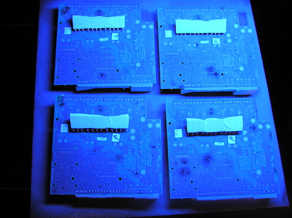
Plasma treatment of the surface of a circuit board before conformal coating

Plasma coating is the application of a nano-coating material onto a surface via a plasma.

Using a jet nozzle the material is supplied to the plasma. Next, the plasma excites the material and this increases the coatings reactivity. This extra reactivity allows the material to optimally cover the surface of the substrate and bond much tighter.

The plasma coating process can be adjusted individually to the substrate. It can be used to coat different materials like metals, glass, ceramics and plastics. These nano coatings can be made to be hydrophobic (water repellent) and hydrophillic (water absorbant) depending on your requirements.

Examples of plasma coating applications include:

  • Improvement of barrier characteristics of plastics for packaging
  • Improved paint application with long-term stability and resulting high flexibility in manufacturing
  • PT Release coatings, for injection molding tools, allow a high number of process cycles without the components having to be stressed with release agents that contain silicone.
  • PT Bond coatings assuring long-term adhesion in the adhesive joint.
  • Corrosion protection coatings that offer extremely high corrosion protection with long term resistance to corrosive electrolytes (especially for aluminum alloys) because of their good barrier effect

Want to know more about plasma coating and protecting your products?

Contact us

Call us on +44 (0) 1226 249019, email your requirements on sales@schservices.com

The ABCs of Plasma Cleaning for Conformal Coating


Plasma cleaning is a process that is gaining more popularity in thin film applications due its highly effective performance on cleaning and modifying surfaces. It is also a highly effective surface cleaning and treatment process before application of conformal coatings.

Plasma circuit treatment of circuit board narrow

What is Plasma?

Plasma is an energy-rich gas state that can be used to modify the surface of a product to improve its performance. This modification can be improving the adhesion of a conformal coating or changing the surface characteristics.

Plasma technology is based on a simple physical principle.

Matter changes its state when energy is supplied to it. Solids become liquid. Liquids become gas.

If additional energy is then fed into a gas by means of electrical discharge it eventually ionises and goes into the energy-rich plasma state, the fourth state of matter.

Plasma is created.

How can Plasma be used for cleaning printed circuit boards?

Plasma treatment can clean, activate or coat nearly all surfaces. These surfaces include plastics, metals, (e.g., aluminum), glass, recycled materials and composite materials. This means the plasma process can be highly effective on many different products.

For electronic circuit surfaces, plasma treatment can be used in two highly effective ways.

That is it can:

  1. Clean the surface of the circuit board to be 100% contamination free. The surface will be free of residues and contamination including release agents and additives.
  2. Activate the surface of the circuit board assembly to allow easier bonding and better adhesion of conformal coatings. It can change the surface energy of the surface to ensure complete adhesion is possible and in some cases it can make materials bond where it was previously impossible.

These properties make it an interesting technique for improving the surface performance of an electronic circuit board.

What are the typical plasma processes available for surface treatment?

There are traditionally three types of plasma treatments.

  • Low-pressure plasma. These plasmas are generated in closed chambers in a vacuum (10-3 to 10-9 bar). They can be used in conjunction with Chemical Vapor Deposition (CVD) coatings like Parylene before application.
  • Corona treatment. Corona treatment (corona process) is a physical process involving high voltage and is mainly used for treatment of films. This is normally not suitable for electronic circuit boards.
  • Atmospheric pressure plasma. Atmospheric plasma is generated under normal pressure. This means that low-pressure chambers are not required. The plasma is created with clean/dry compressed air (plant air) and does not require forming gases. It is possible to integrate plasma directly into manufacturing processes under normal pressure conditions. This is an excellent process for improving adhesion and surface energy performance of circuit boards for conformal coatings.

How is the plasma applied to a circuit board to clean it?

Typical plasma components used for cleaning surfaces on circuits are:

  • Plasma jets (nozzles) to apply the plasma to the surface of the circuit board. They could be controlled by a robotic system.
  • The plasma generators that create the plasma to clean or supply the coatings as required. They provide output power and, in conjunction with complete pretreatment stations, assume various control functions.
  • The process monitoring that controls the nozzles, the movement of the system and the quality of the output.
  • These three parts form the plasma cleaning process.

Want to know more about plasma cleaning and conformal coating performance?

Contact us now, call us on +44 (0) 1226 249019 or email your requirements on sales@schservices.com.


0
  • Your current order total is £0.00 β€” you must have an order with a minimum of £75.00 to place your order.
0
Your Cart
Your cart is empty
  • Your current order total is £0.00 β€” you must have an order with a minimum of £75.00 to place your order.
Calculate Shipping
  • Your current order total is £0.00 β€” you must have an order with a minimum of £75.00 to place your order.

Conformal Coating UK

Technical banner showing PCB and process icons representing conformal coating, masking, inspection and training on the SCH technical knowledge hub.
Conformal Coating UK
Privacy Overview

This website uses cookies so that we can provide you with the best user experience possible. Cookie information is stored in your browser and performs functions such as recognising you when you return to our website and helping our team to understand which sections of the website you find most interesting and useful.