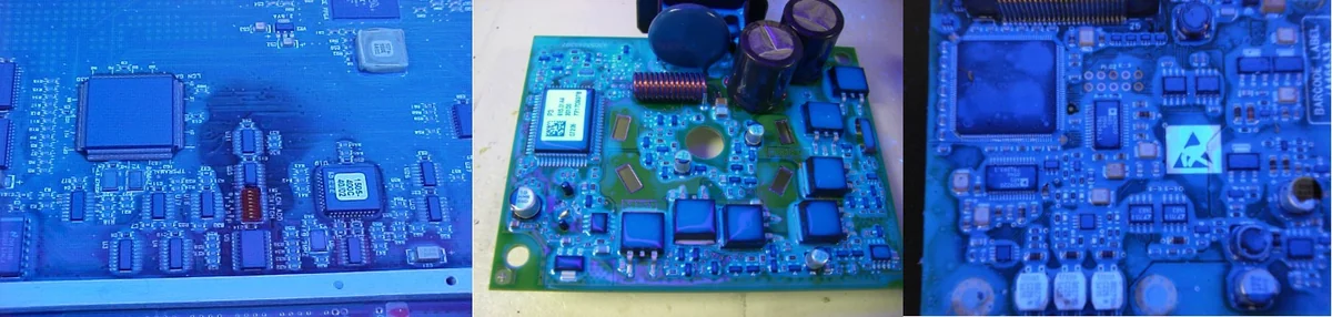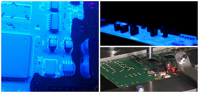
There are several ways to measure the conformal coating thickness on a printed circuit board (PCB). They can be either used on dry or wet film coating.
These techniques include:
- Non-destructive eddy current system
- Micrometer screw gauge
- Wet film gauge
These techniques are explored further below. Alternatively, click through to our article Conformal Coating Thickness Measurement: Wet, Dry & Optical Methods to get a more detailed review.
Non-destructive eddy current system
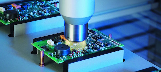
A fast method for measure coating thickness is a system using eddy currents. The process can be extremely quick and accurate to ±1 um.
Using a gauge and flying probe for the measurement the system is extremely easy to use. The process works by placing the test probe head flat on the surface of the conformal coating and the measurement is almost instantaneous. The system provides an immediate repeatable result for thickness measurement of conformal coating.

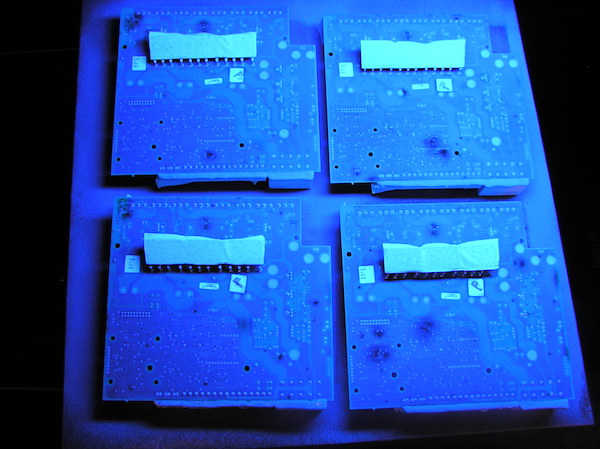
Test coupons are the ideal method for measuring the coating thickness, whether is it spraying or dipping, and can be kept as a physical record of the performance.
Apply the coating to the test coupons at the same time as the circuit board then provides a permanent measurement and an accurate guide to the coating thickness.
There are a couple of issues using a system like this.
First, there needs to be metal in the circuit board directly below the tested point. Otherwise, the system cannot work.
Second, there needs to be a flat area large enough for the test probe. The smallest practical probe is approximately 6mm diameter so any area smaller than this is not practical.
Finally, the surface measured for the probe needs to be flat. If not then there will be errors in the measurement.
Micrometer screw gauge
The low cost method is using a calibrated micrometer screw gauge that can measure down to ± 10 um. First measure a point on the board or test coupon, apply the coating, cure and measure the test coupon again at the same point. The difference gives you the coating thickness.
A couple of pitfalls to avoid are ensuring the coating is cured hard enough since if it is soft it could compact and give a false reading. Also, do not measure one point. Take an average of at least 3 or 4 points since this will give a better result statistically.
Test coupons are the ideal method for measuring the coating thickness, whether is it spraying or dipping, and can be kept as a physical record of the performance.
Wet film gauge
A final method is a wet film measurement technique that is very cost effective.
The technique uses a comb with different size patterns that is placed in the wet coating and the imprint left indicates the wet film thickness. Knowing the solids content of the material means that the material thickness can be calculated.

Need to know more about conformal coating thickness measurement?
Find out more from our article Conformal Coating Thickness Measurement: Wet, Dry & Optical Methods to get a more detailed review.
Or, contact us now and we can discuss how we can help you. Give us a call at (+44) 1226 249019 or email your inquiries at sales@schservices.com