
Parylene Thickness Strategy: Dielectric Performance, Coverage Limits & Cost Control
How to select the right Parylene thickness for reliability, geometry and production efficiency
← Back to the Parylene Process & Reliability Hub
Parylene thickness strategy: how dielectric needs, geometry limits, environmental exposure and cost/throughput trade-offs drive the right micron target.
Parylene Thickness Strategy: How to Choose the Right Micron Target
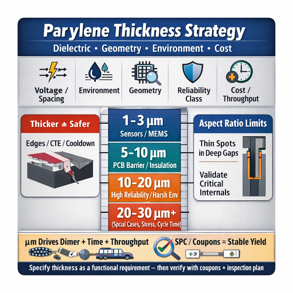
This infographic summarises a practical thickness-selection framework for Parylene coatings. The correct thickness is driven by electrical performance (dielectric margin), environmental exposure (moisture/condensation risk), geometry limits (gaps, cavities and aspect ratio penetration), and mechanical stress/cycle control.
The key message is that thicker is not always better. Extra microns increase dimer consumption, deposition time and stress risk, and do not guarantee improved coverage deep in high-aspect features. The best approach is to specify thickness as a functional requirement, then confirm stability using witness coupons, thickness verification and a documented inspection plan.
Quick Links
Electrical Performance & Dielectric Strength
Parylene offers high dielectric strength per micron. However, voltage stress, creepage distance and geometry all influence required build. Thin films (1–5µm) may be suitable for low-voltage sensors and microelectronics, whereas higher voltage assemblies require greater safety margin.
Electrical spacing design should always be aligned with clearance rules and coating credit strategy. See:
Clearances, Gaps & Encapsulation Rules.
Thickness verification must be controlled via witness coupons and statistical process control:
Thickness Verification (AQL, Coupons & SPC).
Environmental Protection & Moisture Barrier
Barrier performance improves with thickness — but not linearly. After a certain build, incremental benefit reduces relative to cost. Moisture exposure, condensation cycling and ionic contamination must be considered together.
For deeper analysis of environment-driven thickness decisions, see:
Parylene Thickness & Environmental Protection.
Cleaning quality and surface preparation are foundational. Adhesion loss or micro-voids can undermine barrier performance regardless of thickness:
Parylene Cleaning & Adhesion Control.
Geometry Limits: Gaps, Cavities & Aspect Ratio
Parylene is conformal, but vapour transport still follows physics. In high-aspect features, diffusion limits can result in reduced film thickness at the base of narrow cavities. Increasing nominal thickness does not guarantee proportional penetration in deep gaps.
Geometry-driven thin spots are a common root cause of failures. See:
Parylene Defects & Failure Mechanisms.
Design mitigation — vent paths, clearance control and thickness matched to feature depth — should be addressed at layout stage:
Parylene Clearances & Gaps.
Mechanical Stress & Cracking Risk
Thicker films increase internal stress during thermal cycling and cool-down. Sharp edges, CTE mismatch and uncontrolled post-process cooling can increase risk of cracking or flaking.
Thermal management and process stability must be considered alongside thickness decisions. Refer to:
Defects & Mechanical Failure Modes.
Cost Per Micron & Yield Optimisation
Thickness directly impacts:
- Dimer consumption
- Deposition time
- Chamber throughput
- Energy use
- Per-part cost
Excess thickness reduces margin and slows capacity without proportional reliability benefit. Thickness should therefore be specified as a functional requirement, not a “maximum protection” assumption.
Dimer quality and lot traceability also influence stability and yield:
Parylene Dimer Comparison.
Practical Thickness Selection Framework
- Define electrical stress (voltage, spacing, insulation requirement).
- Define environmental exposure (humidity, condensation, salt, chemicals).
- Assess geometry (gaps, cavities, dead ends, high-aspect features).
- Evaluate mechanical stress (thermal cycling, substrate mismatch).
- Balance cost vs incremental reliability gain.
- Validate with coupons, thickness measurement and inspection plan.
Thickness decisions should be validated with structured inspection criteria:
Inspection Acceptance Criteria.
Are You Over- or Under-Specifying Thickness?
Parylene thickness directly affects dielectric performance, coverage reliability, cycle time and material cost. Over-specifying increases cycle time and dimer consumption; under-specifying may compromise long-term performance.
📊 Request a Thickness & Throughput Review – We can evaluate your electrical targets, geometry constraints and production assumptions to define a stable, cost-controlled thickness strategy.
FAQs
Is thicker Parylene always better?
No. Increasing thickness increases cost and mechanical stress risk. Thickness should match electrical, environmental and geometry requirements.
What thickness is typical for PCB protection?
Most PCB applications use 5–15µm depending on voltage, spacing and environment. High-reliability aerospace systems may require thicker films.
How does thickness affect production cost?
Thickness directly increases dimer consumption and deposition time. Over-specification reduces throughput and increases cost per part.
