
Parylene Clearances and Gaps
Design rules for encapsulation, dielectric spacing and vapour penetration
← Back to the Parylene Design Hub
Parylene clearances and gaps play a critical role in determining coating coverage, dielectric performance and long-term reliability. While Parylene is deposited from the vapour phase and is highly conformal, geometry still controls how effectively the coating penetrates gaps, cavities and enclosed features.
This article explains how Parylene clearances and gaps influence encapsulation behaviour, insulation performance and defect risk, and how to design assemblies that coat predictably.
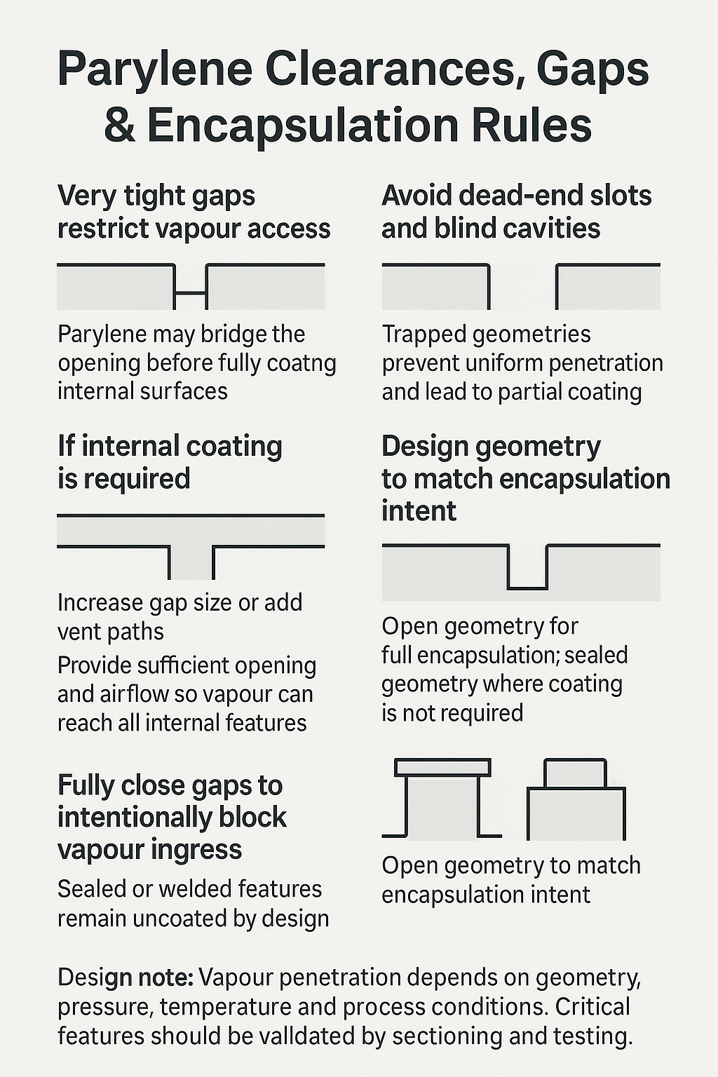
How clearances and gaps control Parylene vapour access, encapsulation and coating reliability.
Why Clearances and Gaps Matter in Parylene Coating
Parylene clearances and gaps affect:
- How deeply vapour penetrates into tight features
- Whether full encapsulation is achieved
- Dielectric strength between conductors
- Risk of voids, thin spots or trapped contamination
Assemblies that ignore Parylene clearance rules often show inconsistent coverage or unexpected electrical failures.
Tight Gaps, Open Gaps & Dead-End Cavities
Different gap types behave very differently during coating:
- Very tight gaps may limit vapour penetration and effective thickness
- Optimised gaps allow uniform coating and predictable insulation
- Dead-end cavities can trap contaminants and restrict vapour flow
Good Parylene design favours vented, accessible geometries wherever possible.
Encapsulation vs Partial Coverage
Designers must decide whether full encapsulation is required or whether partial coverage is acceptable.
- Full encapsulation improves environmental protection
- Partial coverage may be sufficient for some electrical insulation needs
- Encapsulation intent should be defined early in the design process
Clear communication of encapsulation intent is essential when specifying Parylene clearances and gaps.
Electrical Clearances & Dielectric Performance
Electrical spacing rules depend on:
- Operating voltage and environment
- Parylene type and coating thickness
- Surface condition and geometry
While Parylene offers excellent dielectric strength, it should not be used to compensate for fundamentally poor electrical design.
Common Clearance Design Pitfalls
Typical clearance-related issues include:
- Unvented slots and blind holes
- Sharp internal corners that concentrate stress
- Assuming uniform thickness in inaccessible regions
Applying proven Parylene clearances and gaps guidelines reduces defect risk and improves reliability.
Parylene on Wikipedia.
Explore Topic Hubs
Why Work with SCH on Parylene Clearance Design?
SCH supports customers applying Parylene clearances and gaps guidelines through:
- Design-led reviews focused on geometry, access and encapsulation intent
- Turnkey capability covering coating services, equipment and materials
- Cross-sector experience in medical, aerospace, automotive and industrial electronics
- Clear scale-up pathways from prototype to production
Call: +44 (0)1226 249019 · Email: sales@schservices.com
Contact SCH to discuss clearance and encapsulation design ›
Disclaimer: This article provides general guidance on Parylene design. Performance, suitability and compliance depend on the specific design, materials and environment. SCH Services can review assemblies and specifications to confirm the most appropriate Parylene coating approach.
