Mon - Thur 7.30-15.30   Fri 7.30-14.00

Hybrid ALD/CVD Coatings for LED Protection – Where Do They Really Fit?


Understanding the role of ultra-thin coatings in LED protection without the hype

Protecting LEDs from long-term exposure to harsh environments is becoming increasingly critical, particularly for outdoor and high-reliability applications. Moisture, salt, UV exposure and thermal cycling all create failure risks that must be managed through coating selection.

There are already multiple established protection strategies including Parylene, liquid conformal coatings, ultra-thin fluoropolymers and encapsulation. Each offers advantages, but all involve trade-offs between protection level, process complexity, optical performance and cost.

Hybrid ALD (Atomic Layer Deposition) / CVD (Chemical Vapour Deposition) coatings are often presented as a new alternative. The key question is not whether they are interesting, but where they realistically fit alongside existing coating technologies.

What is a Hybrid ALD/CVD Coating?

Hybrid coatings combine two thin-film deposition techniques into a layered structure.

  • CVD (used in Parylene) deposits a conformal coating in a vacuum environment
  • ALD deposits extremely thin, controlled layers at atomic scale

In hybrid systems, these layers are applied sequentially to build a multi-layer film. The structure is fundamentally different from traditional coatings, as properties can be engineered layer-by-layer rather than relying on a single material.

The result is an ultra-thin coating system, typically in the nanometre range, with tailored barrier, adhesion and surface properties.

Compare this with traditional coating approaches β†’

Why is this approach relevant for LEDs?

LED protection introduces constraints that are not always present in standard PCB coating.

  • Optical clarity – coatings must not reduce light output
  • UV stability – long-term outdoor exposure
  • Moisture resistance – prevention of corrosion and failure
  • Thermal stability – cycling and elevated temperatures

Hybrid coatings are often positioned as suitable because they are extremely thin, highly transparent and can provide good barrier performance relative to thickness.

In applications where traditional coatings create optical or masking challenges, this type of approach becomes more attractive.

Masking Reduction – Not Elimination

One of the most common claims is that hybrid coatings do not require masking due to their extremely low thickness.

Reality check: Ultra-thin coatings can reduce masking requirements, but they do not remove interface risks completely. Connectors, contact surfaces and critical electrical interfaces still require validation.

Whether masking can be reduced depends on:

  • Connector design and contact force
  • Electrical sensitivity of interfaces
  • Long-term wear and fretting behaviour
  • Customer acceptance criteria

In practice, masking strategy becomes an engineering decision rather than being eliminated entirely.

Performance Compared to Established Coatings

Hybrid coatings are often compared with Parylene and liquid conformal coatings. The comparison is not simply performance-based, but application-dependent.

  • Hybrid coatings – ultra-thin, optically clear, engineered film structure
  • Parylene – proven barrier performance and long-term reliability
  • Liquid coatings – scalable, robust and well understood processes

Hybrid coatings can offer advantages in specific LED applications, particularly where optical performance is critical. However, established coatings still dominate in many applications due to proven reliability and process maturity.

The decision is not which coating is β€œbest”, but which is most appropriate for the application and risk profile.

Process and Cost Considerations

Hybrid ALD/CVD processes are often described as low cost due to reduced masking and simple operation. However, real cost depends on the full system.

  • Equipment investment and process control requirements
  • Throughput and batch size limitations
  • Cycle time and scalability
  • Validation and qualification requirements

While operator interaction may be simple, the overall process must be evaluated at production scale rather than individual step level.

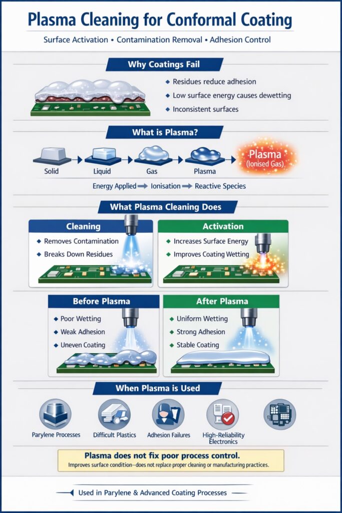
For surface preparation prior to coating, see plasma cleaning for conformal coating, which explains how plasma is used to improve adhesion and surface energy.

Where Hybrid Coatings Actually Fit

From a practical engineering perspective, hybrid ALD/CVD coatings are best positioned as a specialist solution rather than a universal replacement.

  • Suitable for optically sensitive applications such as LEDs
  • Useful where ultra-thin coatings provide a design advantage
  • Complementary to existing coating technologies

For most applications, coating selection remains driven by environment, geometry, process capability and reliability requirements.

In many cases, structured coating strategies using established materials remain the most robust approach.

Final Perspective

Hybrid ALD/CVD coatings represent a technically interesting development, particularly for LED protection where optical and environmental requirements must be balanced.

However, they should be viewed as part of a broader coating strategy rather than a direct replacement for Parylene or conformal coatings.

The key is selecting the right coating approach for the application, not chasing a single β€œbest” material.

Need support selecting the right coating approach?

SCH supports coating selection, process design and validation across conformal coatings, Parylene and hybrid strategies.

Contact us to discuss your application.

↑ Back to top

Note: This article provides general technical guidance only. Final design, safety and compliance decisions must be validated against application requirements and relevant standards.

What are conformal coating masking boots and how can they save you money?


The use of masking materials such as tapes, dots and liquid latex can be a highly effective process in protecting components from ingress of conformal coating. However, the masking process can be labour intensive, difficult and time consuming.

Using reusable, custom masking boots offers a labour saving alternative in both the masking and de-masking stages of the coating process. This can save you lots of time and money.

Conformal coating masking boots used on Printed circuit board as an alternative to masking tapes

Three simple reasons why conformal coating masking boots can save you money

  • Masking time is reduced. Using masking boots as an alternative can be 4-5 times quicker than masking tape.
  • De-masking time is reduced. Again it is much quicker to remove masking boots than tape
  • Masking boots don’t leak as easily as tape. So there is less chance of a need to repair or remove leaked coating.

This means you can save a lot of money very quickly when switching to custom masking boots.


How Diamond MT saved nearly 60% of their process time switching to masking boots

Diamond MT, a conformal coating and Parylene coating service provider, found they saved 60% of their current costs by switching to the SCH range of conformal coating masking boots.

Sean Horn, Diamond MT, explains how they did it.

β€œWe had initially wanted to try SCH’s conformal coating masking boots for price savings. However, once we began to work with Lee on our specific masking application, we realised that we could extend the life of our boots over 200%. We switched immediately!

We then realised the importance of working with someone who understands conformal coatings. We will not being going back to our previous supplier.”

Sean Horn, Director, Diamond MT, Parylene and conformal coating subcontract service provider.


Request Your Free Masking Sample Pack

You can experience the quality of our masking solutions first-hand by requesting a free sample pack. The pack includes a selection of our masking tapes, dots, boots and pre-cut shapes, allowing you to test their performance directly in your coating process. It’s a quick and risk-free way to see how our materials ensure clean removal, precise coverage, and time-saving application.

πŸ‘‰ Contact us today to request your free sample pack and find the right masking solution for your production needs.


Find out how much you can save by switching to custom boots

We are happy to provide a quotation for our masking boots so you can see for yourself how much you can save.

Just provide us with three pieces of information:

  • Provide a picture of the board you wish to test
  • Identify the components you need to mask
  • Provide the component identification codes (manufacture details etc)

Contact us today to request your quotation for conformal coating masking boots. Call us on +44 (0) 1226 249019, email your requirements on sales@schservices.com

What is Plasma Coating?


Where plasma-deposited nano films fit in surface engineering and electronics protection

Plasma coating is a surface treatment process in which a reactive coating precursor is introduced into a plasma and deposited onto a substrate as an ultra-thin functional film. It is typically used where very low film thickness, tailored surface behaviour or specialist adhesion performance is required.

In practical terms, plasma coating is not the same as traditional conformal coating and it is not the same as Parylene deposition. It belongs more to the world of surface engineering, where the goal is often to modify how a surface behaves rather than build a thick physical barrier.

That makes plasma coating interesting, but also easy to misunderstand. The key question is not whether it is advanced, but where it actually fits and what problems it is designed to solve.

Plasma treatment of the surface of a circuit board before conformal coating

How plasma coating works

In a plasma coating process, a precursor material is introduced into a plasma zone, often through a jet nozzle or controlled gas-phase system. The plasma activates the chemistry, increasing its reactivity and allowing it to bond to the substrate surface more effectively.

This process can be adjusted for different materials including metals, glass, ceramics and plastics. Depending on the chemistry used, the resulting film can be tailored to create different surface properties such as water repellence, improved adhesion or barrier enhancement.

Because the film is extremely thin, plasma coating is usually used to change surface function rather than build the kind of thick protective layer associated with conventional conformal coatings.

Important: Plasma coating should not be confused with plasma surface preparation. Plasma preparation activates or cleans a surface before coating, while plasma coating deposits a functional film onto the surface itself.

What plasma coatings can do

Plasma-deposited coatings are typically used to alter surface behaviour in a very targeted way. Depending on the chemistry and process design, they can be made hydrophobic or hydrophilic and can improve how a surface performs in later manufacturing or service.

  • Barrier improvement for selected plastic or functional surfaces
  • Adhesion improvement for bonding or paint application
  • Release properties for tooling and mould-related applications
  • Corrosion resistance support where ultra-thin barrier behaviour is beneficial
  • Surface energy modification to improve how a material interacts with liquids, adhesives or later coatings

These are specialist functions. They are not direct equivalents to the role of a conventional PCB conformal coating.

Where plasma coating fits in electronics

In electronics, plasma coating is best understood as a niche or specialist surface engineering option rather than a mainstream replacement for conformal coating. It may be relevant where very thin deposited functionality is needed, but it does not automatically replace the insulation, thickness or physical protection provided by traditional coating systems.

That is why it is important to compare it in the right way. If the real need is full electrical insulation, environmental barrier performance or robust film build, then conventional conformal coatings or Parylene may still be the more appropriate technologies.

For a broader comparison of established protection strategies, see Parylene vs Conformal Coating: How to Choose the Right Protection for Electronics.

What plasma coating does not replace

Plasma coating is often interesting because it is thin, highly engineered and flexible at surface level. But those same features also mean it should not be overstated.

  • It does not automatically replace conformal coating where thickness and dielectric protection are required
  • It does not automatically replace Parylene where true conformal vapour-deposited coverage is needed
  • It does not remove the need for proper process selection, testing and validation

Like other advanced thin-film technologies, it is best viewed as a specialist tool for specific problems rather than a universal answer.

Reality check: If the requirement is mainstream PCB protection in a harsh environment, plasma coating is usually not the first question to ask. The first question is what level of barrier, insulation, coverage and process control the product actually needs.

Final perspective

Plasma coating is a legitimate and highly specialised surface engineering technology. Its value lies in controlled surface modification, ultra-thin deposited functionality and application-specific performance tuning.

For most electronics users, the important thing is understanding where it fits relative to better-known technologies such as conformal coating and Parylene. The goal is not to use the most advanced process available, but to select the process that matches the product, environment and manufacturing reality.

If you are trying to choose between different protection strategies, it is usually better to start with the function required and then work back to the most appropriate coating technology.

Need help reviewing a coating or surface protection problem?

SCH supports customers with coating selection, process review and technical guidance across conformal coating, Parylene and specialist protection strategies.

Contact us to discuss your application.

↑ Back to top

Note: This article provides general technical guidance only. Final design, process and compliance decisions must be validated against the actual substrate, coating chemistry and application requirements.

The ABCs of Plasma Cleaning for Conformal Coating


How plasma treatment improves adhesion, surface energy and coating reliability

Surface condition is one of the biggest drivers of coating success or failure.

Even when the correct conformal coating is selected, poor adhesion, dewetting and long-term reliability issues often trace back to contamination or low surface energy at the substrate level.

Plasma cleaning provides a controlled way to remove contamination and modify surface energy before coating. It is widely used where conventional cleaning alone cannot deliver consistent adhesion β€” particularly for difficult substrates and high-reliability applications.

Emerging ultra-thin coating technologies such as hybrid ALD/CVD coatings reduce reliance on traditional masking and surface preparation, but still depend on controlled surface conditions to perform reliably.

Plasma cleaning infographic showing contamination removal, increased surface energy and improved wetting for conformal coating adhesion on PCB assemblies

Plasma cleaning improves coating adhesion by removing contamination and increasing surface energy, enabling uniform wetting and reliable conformal coating performance on PCB assemblies.

What is plasma?

Plasma is often described as the fourth state of matter. When sufficient energy is applied to a gas, it becomes ionised, forming an ΰ€Šΰ€°ΰ₯ΰ€œΰ€Ύ-rich environment containing ions, electrons and reactive species.

This reactive environment allows plasma to interact with surfaces at a molecular level.

In coating processes, plasma is used to clean, activate or modify surfaces without mechanical contact or liquid chemistry.

Why plasma cleaning is used before conformal coating

Plasma treatment addresses two key challenges in coating processes:

  • Removal of contamination – including organic residues, oils, additives and weak surface films
  • Surface activation – increasing surface energy to improve coating wetting and adhesion

This is particularly important where coatings struggle to wet or bond consistently. For the wider context of how cleanliness affects coating reliability, see surface preparation and cleanliness for conformal coating.

Reality check: Plasma does not fix poor process control. If contamination levels are inconsistent or excessive, plasma may improve results but will not stabilise an unstable upstream process.

What plasma does to a PCB surface

When applied to electronic assemblies, plasma treatment can:

  • Remove organic contamination at a molecular level
  • Increase surface energy to improve wetting
  • Promote stronger adhesion between coating and substrate
  • Enable bonding on otherwise difficult materials

This makes it particularly useful for Parylene processes and difficult-to-bond substrates where adhesion is a known risk.

Types of plasma processes used

There are three main plasma approaches used in surface treatment:

  • Low-pressure plasma: Vacuum-based systems used for high control and uniform treatment. Often used in conjunction with vapour deposition processes such as Parylene.
  • Atmospheric plasma: Operates at normal pressure using compressed air. Easier to integrate inline and widely used for PCB surface activation.
  • Corona treatment: Primarily used for films and packaging materials. Generally not suitable for complex PCB assemblies.

Atmospheric plasma is typically the most practical option for conformal coating processes due to ease of integration and process flexibility.

How plasma is applied in practice

A typical plasma treatment system consists of:

  • Plasma jet or nozzle: directs the plasma onto the PCB surface
  • Generator: creates and controls the plasma energy
  • Motion system: ensures consistent coverage across the assembly
  • Process control: manages power, exposure time and repeatability

These systems are often integrated into automated lines or used as standalone pre-treatment steps.

Where plasma cleaning fits in the process

Plasma is not a universal requirement. It is typically used where standard cleaning and process control are not sufficient.

  • Difficult substrates (plastics, low surface energy materials)
  • High-reliability coating requirements
  • Parylene coating processes requiring adhesion control
  • Situations where dewetting or adhesion failure has been observed

For most standard conformal coating processes, stable cleaning and handling control are often sufficient without plasma.

In complex assemblies where adhesion, geometry and coating boundaries interact, plasma is often part of a wider process strategy rather than a standalone solution. See hybrid coating strategies for complex PCB assemblies.

Summary

Plasma cleaning is a powerful surface preparation tool, but it is not a substitute for good process control.

  • Improves adhesion and surface energy
  • Removes contamination at a molecular level
  • Supports difficult coating applications
  • Best used where standard processes cannot deliver stability

Used correctly, plasma can significantly improve coating reliability. Used incorrectly, it can mask underlying process problems without resolving them.

Why Choose SCH Services?

SCH Services supports coating processes with practical engineering input β€” from surface preparation and adhesion control through to coating selection, process development and validation.

  • ✈️ 25+ Years of Expertise
  • πŸ› οΈ Process-Led Support
  • πŸ“ˆ Scalable Solutions
  • 🌍 Global Support
  • βœ… Focus on Real Process Stability

πŸ“ž Call: +44 (0)1226 249019 | βœ‰ Email: sales@schservices.com | πŸ’¬ Contact Us β€Ί

↑ Back to top

Note: This article provides general technical guidance only. Final process decisions should be validated against the specific assembly, materials and applicable standards.

0
  • Your current order total is £0.00 β€” you must have an order with a minimum of £75.00 to place your order.
0
Your Cart
Your cart is empty
  • Your current order total is £0.00 β€” you must have an order with a minimum of £75.00 to place your order.
Calculate Shipping
  • Your current order total is £0.00 β€” you must have an order with a minimum of £75.00 to place your order.

Conformal Coating UK

Technical banner showing PCB and process icons representing conformal coating, masking, inspection and training on the SCH technical knowledge hub.
Conformal Coating UK
Privacy Overview

This website uses cookies so that we can provide you with the best user experience possible. Cookie information is stored in your browser and performs functions such as recognising you when you return to our website and helping our team to understand which sections of the website you find most interesting and useful.