Parylene Coating Applications: Where Parylene Excels
High-reliability electronics, medical and harsh-environment applications
← Back to the Parylene Basics Hub
Quick Links
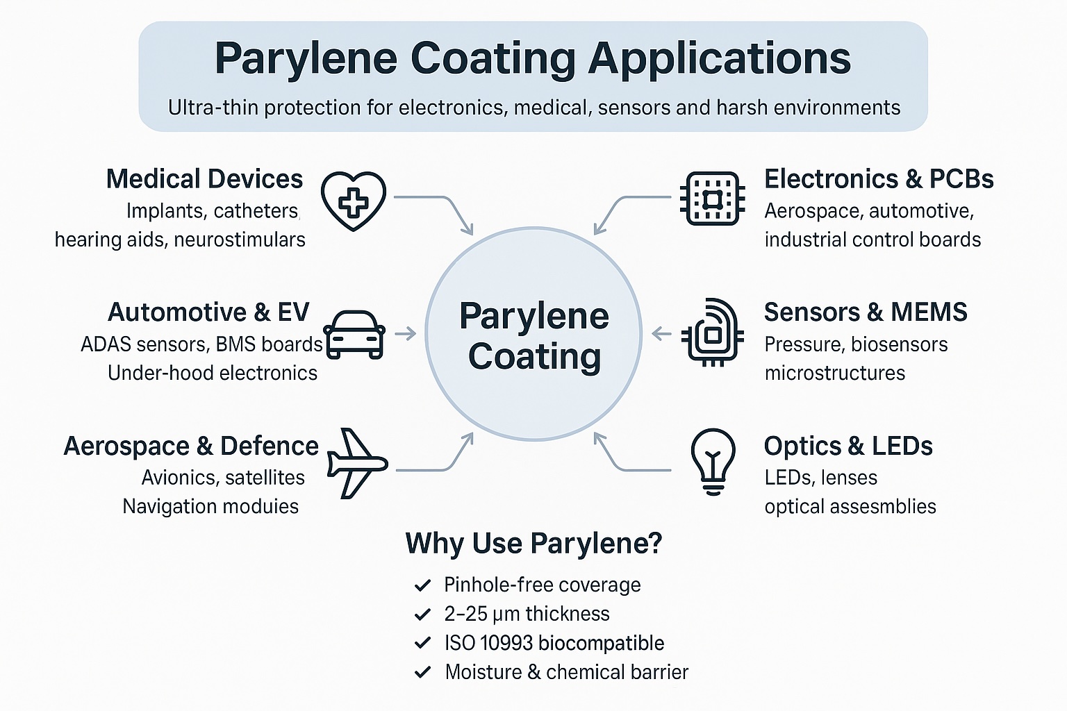
Electronics & PCBs
Parylene’s vapour-phase polymerisation produces uniform films over complex 3D assemblies, offering exceptional moisture/ionic barrier, dielectric strength, and creepage/clearance support without trapped solvents.
- High-reliability assemblies: aerospace, medical, industrial controls, marine and defence electronics.
- Fine-pitch & dense boards: under-component coverage and fillet protection where liquid coatings struggle.
- Corrosive environments: salt fog, humidity/condensation cycling, pollution exposure.
Typical approach: 10–25 µm Parylene C for general reliability; consider Parylene F (HT) for higher temperature or enhanced chemical resistance. Validate thickness with optical thickness measurement and manage via AQL/SPC plans.
Medical Devices & Implants
Parylene is widely used for biocompatible, ultra-thin encapsulation where flexibility, low modulus and chemical purity matter.
- Implantable electronics: neurostimulation, cardiac monitoring, micro-leads, sensors.
- Minimally invasive tools & catheters: lubricity, moisture barrier, electrical isolation.
- Diagnostic and wearable devices: thin, conformal insulation without adding weight or stiffness.
Typical approach: 5–15 µm where extreme thinness and flexibility are required; Parylene N for best dielectric at minimal thickness, Parylene C for general barrier performance. Confirm adhesion with appropriate surface prep and silanes (e.g., A-174).
Sensors, MEMS & RF
For microstructures and moving elements, Parylene’s line-of-sight-independent deposition ensures coverage inside cavities and around sharp topography.
- MEMS & micro-actuators: thin passivation without stiction from solvents.
- Pressure, humidity & gas sensors: barrier vs. contamination while maintaining response.
- RF & antennas: low-loss dielectric over fine conductors; choose grade for dielectric constant needs.
Typical approach: 2–10 µm films for minimal mass loading; Parylene N when lowest dielectric constant is preferred; validate with coupon mapping and SPC.
Optics, LEDs & Displays
Parylene offers transparent, low-stress encapsulation for optical assemblies and LEDs, protecting against moisture and corrosion without yellowing when the correct grade and exposure limits are observed.
- LED modules: moisture barrier around wire bonds and phosphors.
- Opto-electronics: thin, uniform encapsulation of lenses, light pipes and sensors.
- Display sub-assemblies: localised protection of sensitive regions and interconnects.
Typical approach: 5–15 µm, grade selection per optical and thermal demands. Verify masking quality at windows/keep-outs under magnification.
Aerospace, Automotive & Harsh Environments
When exposed to thermal cycling, salt fog, fuels, oils and condensation, Parylene’s pinhole-free film and strong adhesion deliver long-term protection.
- Aerospace & defence: mission-critical electronics, sensors and interconnects.
- Automotive/EV: under-hood electronics, BMS/pack controls, ADAS sensors.
- Industrial & marine: drives, encoders, power modules in corrosive atmospheres.
Typical approach: 15–30 µm Parylene C as default barrier; consider Parylene F for elevated temperature and chemical mix exposure. Control masking strategy for connectors and vents.
Plastics, Elastomers & Metals
Parylene adheres well to many substrates with the right surface preparation.
- Plastics: PC, ABS, PA, PEEK, PPS, PEI; use plasma + silane for low-energy plastics (e.g., PE, PP, PTFE blends).
- Elastomers: seals, gaskets, catheter shafts—thin films for barrier/lubricity without stiffening.
- Metals: Al, Cu, Ni, stainless; clean oxide/organics to ensure robust adhesion.
Typical approach: Validate adhesion on coupons per material variant; start at 5–15 µm and tune per barrier need and flexibility.
Barrier Packaging & Specialty Uses
Ultra-thin Parylene layers can reduce permeation and improve cleanliness for specialty packaging or precision parts.
- Moisture/oxygen barrier: sensitive components, test coupons, labware.
- Friction & anti-stiction surfaces: low surface energy for moving interfaces.
- Chemical splash resistance: localised protection on fixtures and tools.
Typical approach: 1–5 µm for packaging films and low-mass parts; verify barrier via application-specific tests.
Selection Guide: Grade & Thickness
| Application Need | Recommended Grade | Typical Thickness | Notes |
|---|---|---|---|
| General electronics barrier | Parylene C | 10–25 µm | Good moisture/ionic barrier and dielectric strength. |
| Ultra-thin dielectric / low Dk | Parylene N | 2–10 µm | Lowest dielectric constant; great for MEMS/RF. |
| Higher temp / chemicals | Parylene F (HT) | 10–30 µm | Thermal & chemical robustness; review cost impact. |
| Flexing parts / elastomers | C or N | 5–15 µm | Balance barrier vs. flexibility; validate bend tests. |
Convert target thickness to dimer mass via your chamber calibration and verify with optical thickness meters. Use AQL/coupon/SPC to control uniformity across the load.
Guidance on how thickness influences moisture protection, condensation resilience and environmental durability is explained in our Parylene thickness guide.
Design & Keep-Outs for Parylene
- Masking for vacuum: choose robust reusable boots, tapes, dots or custom shapes.
- Adhesion prep: clean, plasma activate low-energy plastics, then apply silanes (e.g., A-174) where compatible.
- Vents & moving parts: define keep-outs and breathable pathways to avoid sealing vents unintentionally.
- Fixtures: rack parts for line-of-sight and diffusion; avoid shadowing and pocketing.
Inspection & Verification
- Coverage & edges: inspect under magnification, confirming keep-outs and mask lines.
- Thickness: verify on witness coupons and critical locations using optical methods or validated proxies.
- Defects: document and trend pinholes, edge creep, adhesion loss; feed back into cleaning/prep.
- Inspection Criteria: IPC-A-610 test methods.
For a process overview, see Parylene Deposition: Process Parameters.
Why Choose SCH Services?
Partnering with SCH Services means more than just outsourcing — you gain a complete, integrated platform for
Conformal Coating, Parylene & ProShieldESD Solutions, alongside equipment, materials, and training, all backed by decades of hands-on expertise.
- ✈️ 25+ Years of Expertise – Specialists in coating technologies trusted by aerospace, medical, defence, automotive, and electronics industries worldwide.
- 🛠️ End-to-End Support – Guidance on coating selection, Parylene grades, masking strategies, application methods, inspection, and ProShieldESD integration.
- 📈 Scalable Solutions – From small prototype batches to full-scale, high-volume production, SCH delivers flexible capacity that grows with your needs.
- 🌍 Global Reach – Responsive technical support and supply coverage across Europe, North America, and Asia.
- ✅ Proven Reliability – A strong reputation built on quality, consistency, and customer satisfaction across services, equipment, and materials.
📞 Call: +44 (0)1226 249019
✉ Email: sales@schservices.com
💬 Contact Us ›
