
Parylene Thickness Specification Guide: Dielectric Performance, Coverage Limits & Cost Control
How to Specify the Correct Parylene Coating Thickness
Choosing the correct Parylene coating thickness is one of the most important engineering decisions in a conformal coating process. Too thin and the coating may not deliver the required environmental protection. Too thick and the coating increases cost, cycle time and mechanical stress.
Unlike liquid coatings, Parylene forms a uniform molecular film deposited by vacuum chemical vapour deposition (CVD). This means protection can often be achieved at far thinner thicknesses than traditional coatings.
This guide explains how engineers specify Parylene coating thickness in real production environments, balancing dielectric performance, environmental protection, geometry coverage and process efficiency.
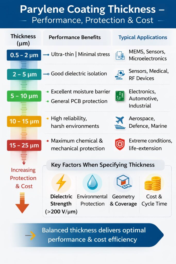
Typical Parylene coating thickness ranges from ultra-thin 0.5 µm films used in MEMS devices through to 25 µm layers used in high-reliability aerospace and defence electronics.
🔗 Quick Navigation
Typical Parylene Coating Thickness Ranges
Although Parylene can be deposited from nanometres to tens of microns, most electronics applications fall within a relatively narrow range.
Because Parylene coatings are pinhole-free and conformal, effective protection is often achieved at significantly thinner thickness than liquid coatings.
Thickness vs Dielectric Performance
Parylene is widely used as an electrical insulation layer due to its high dielectric strength.
- Parylene C dielectric strength ≈ 200 V per micron
- A 10 µm coating can therefore withstand approximately 2 kV
This means relatively thin coatings can provide strong electrical insulation for sensors, connectors and high-density electronics.
For applications requiring high dielectric isolation, engineers may choose Parylene N due to its lower dielectric constant and excellent electrical properties.
Thickness vs Environmental Protection
Environmental protection improves with thickness, but not linearly.
Key protection mechanisms include:
- Moisture barrier performance
- Chemical resistance
- Mechanical durability
For most electronics applications:
- 5–10 µm provides excellent moisture protection
- 10–20 µm may be required for aggressive environments
Increasing thickness beyond this level often delivers diminishing returns while increasing process cost.
Coverage Limits and Geometry Effects
Because Parylene deposits from a vapour phase, coating thickness remains highly uniform across complex assemblies.
However geometry still influences coating performance.
Examples include:
- Deep cavities where deposition rate slows
- Shadowed regions behind tall components
- High-aspect-ratio gaps between components
Proper design, fixturing and masking strategies help ensure uniform coating thickness across the entire assembly.
Thickness vs Cost and Process Throughput
Coating thickness has a direct impact on process economics.
Increasing thickness increases:
- Dimer consumption
- Deposition cycle time
- Production cost
For example:
- 5 µm coating may deposit in ~1 hour
- 20 µm coating may require significantly longer process time
For high-volume manufacturing, selecting the minimum thickness that meets performance requirements can significantly improve production efficiency.
Companies developing in-house coating capability often combine this optimisation with the correct Parylene deposition equipment to achieve predictable throughput and process stability.
How Engineers Specify Parylene Thickness
Rather than specifying a single number, engineers typically specify a thickness range.
Example specification:
Parylene C – 10–15 µm
This allows process variation while ensuring the coating meets functional requirements.
Typical specification considerations include:
- Electrical insulation requirements
- Environmental protection targets
- Component geometry
- Manufacturing throughput
For projects where the correct thickness is uncertain, many manufacturers begin with coating trials to determine optimal performance before production.
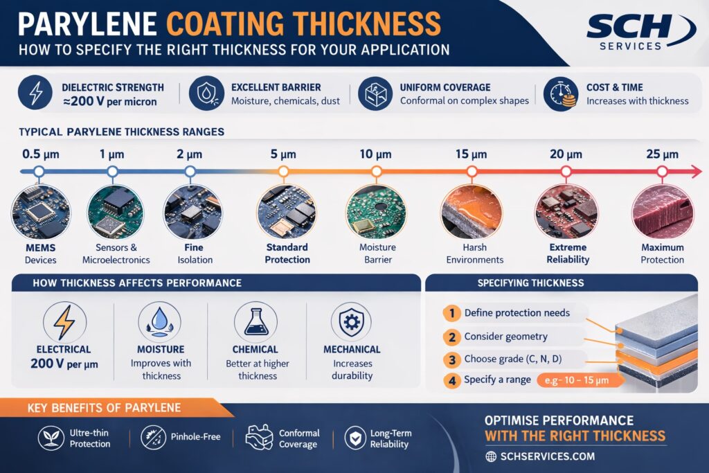
Engineering guide illustrating how Parylene coating thickness influences dielectric strength, moisture barrier performance, coverage of complex geometries and overall coating cost.
Parylene Coating Trials & Process Development
If you are developing a new Parylene application, coating trials can help determine the optimal thickness and coating grade.
SCH provides support including:
- Subcontract Parylene coating services
- Process trials and validation
- Equipment supply and training for in-house coating
FAQs
What is the typical thickness of Parylene coating?
Most electronics applications use coatings between 5 and 15 microns depending on environmental protection requirements.
Can Parylene coatings be extremely thin?
Yes. Parylene can be deposited at sub-micron thickness for MEMS and sensor applications.
Does thicker Parylene provide better protection?
Protection generally increases with thickness, but benefits diminish beyond certain levels and cost increases significantly.
Related Parylene Resources
Why Choose SCH Services?
Partnering with SCH means gaining a complete, integrated platform for Conformal Coating, Parylene & ProShieldESD with equipment, materials, and training, backed by decades of expertise.
- ✈️ 25+ Years – trusted worldwide
- 🛠️ End-to-End Support – coating, masking, application, inspection
- 📈 Scalable Solutions – prototypes to high-volume
- 🌍 Global Reach – support in EU, NA, Asia
- ✅ Proven Reliability – consistent quality & service
📞 Call: +44 (0)1226 249019 | ✉ Email: sales@schservices.com | 💬 Contact Us ›
