
Parylene Thickness & Environmental Protection: How Much Is Enough?
Parylene thickness is one of the first things engineers ask about — and one of the easiest specs to get wrong. Too thin, and you may not achieve the environmental durability margin you need. Too thick, and you add cost, deposition time, and unnecessary build-up in tight features.
This article explains how thickness relates to real-world performance, especially for moisture protection, condensation resilience, and water exposure. It also provides sensible thickness bands you can use for early-stage specification — before committing to trials or a production thickness window. For engineers moving from general guidance to a formal requirement, see our Parylene Thickness Specification Guide.
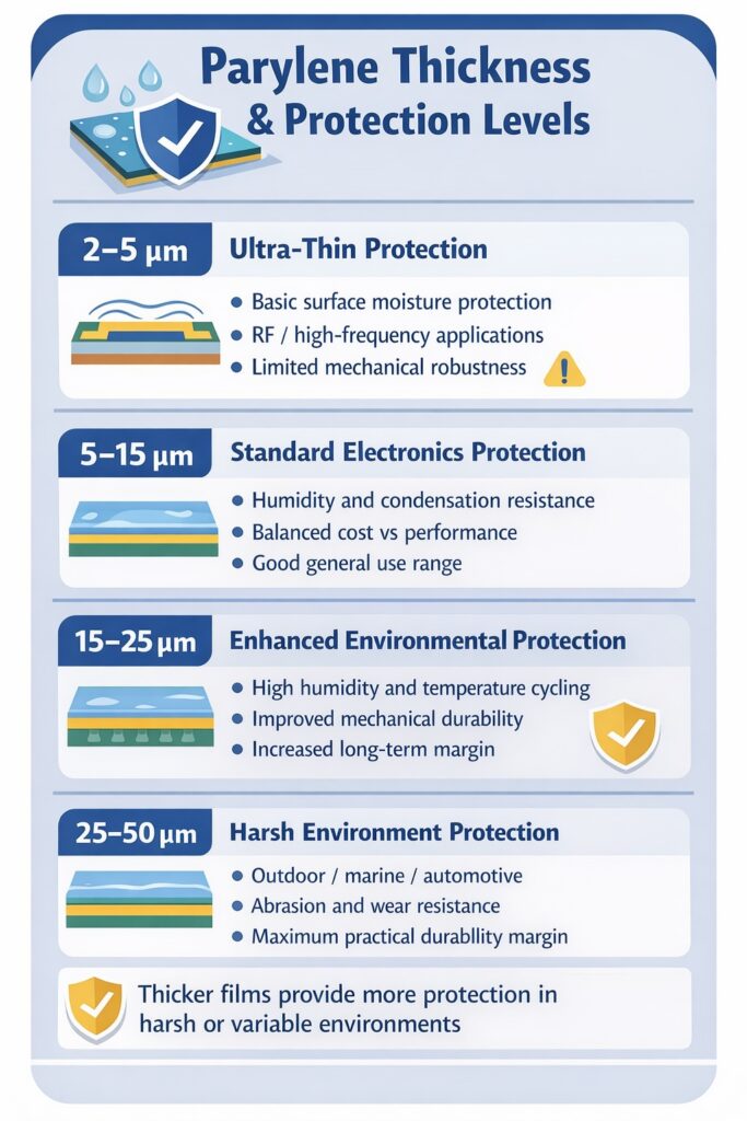
Typical Parylene thickness bands (µm) and how environmental protection margin increases with thickness.
Related Knowledge Hubs:
The key idea: thickness increases durability margin, not just “barrier”
Parylene is deposited by CVD (Chemical Vapour Deposition) and forms an exceptionally conformal polymer film. In clean, controlled conditions, even thin Parylene can provide excellent dielectric and moisture-barrier characteristics.
However, in real products the dominant failure modes are rarely “bulk material permeability” alone. Thickness helps because it improves:
- Resistance to micro-damage from handling, abrasion, vibration and assembly interfaces
- Condensation cycling tolerance (wet/dry cycling stresses coatings at edges, corners and interfaces)
- Edge coverage robustness and stability around sharp features
- Time-to-ingress margin for moisture diffusion and ionic activation mechanisms
Takeaway: Parylene thickness is a reliability and risk decision as much as a “barrier” decision.
Typical Parylene thickness bands (µm) and what they’re used for
2–5 µm: ultra-thin protection (dimension / RF-sensitive builds)
- Basic surface moisture protection and insulation improvement
- Low added mass and minimal dimensional impact
- Often used where dielectric loading must be minimised (RF / high frequency)
Limitations: lower mechanical robustness and reduced tolerance to abrasion, handling damage, and harsh condensation cycling.
5–15 µm: typical electronics protection (balanced default range)
- Strong humidity resistance and condensation protection for many industrial environments
- Good balance of cost, build-up control and performance
- Common range used when you want a sensible “first pass” specification
Best for: general industrial electronics, controlled outdoor enclosures, assemblies where contamination control is good.
15–25 µm: enhanced environmental durability (more margin)
- Higher humidity exposure, more aggressive temperature cycling
- Improved robustness at edges, corners, interfaces and around component bodies
- Often selected when long service life matters more than minimal coating mass
Best for: demanding industrial environments, higher reliability builds, long-life field products.
25–50 µm: harsh environments (maximum practical durability margin)
- High reliability applications where environmental margin is prioritised
- Improved tolerance to handling and mechanical wear over time
- More deposition time and higher cost — so should be justified by environment and duty cycle
Best for: marine / salt-rich atmospheres, harsh outdoor exposure, high-risk reliability targets.
Moisture & water exposure: what improves as thickness increases?
Engineers often assume “thicker = waterproof”. In reality, it’s more accurate to think in terms of risk reduction and time-to-failure margin.
Increasing thickness typically improves:
- Resistance to local defects (a thicker film is harder to compromise at a single point)
- Survivability under condensation cycles where wet/dry repetition stresses interfaces
- Mechanical durability in handling and assembly (especially at edges and sharp features)
- Environmental margin when there is uncertainty in actual field exposure
Important nuance: performance does not increase linearly. A 20 µm coating is not “four times better” than 5 µm — but it can be significantly more forgiving in harsh or variable environments.
What usually drives moisture-related failures (and why thickness helps)
Moisture-related failures in electronics are often triggered by a combination of:
- Condensation (liquid water films are far more aggressive than “humidity”)
- Ionic residues / contamination enabling electrochemical migration
- Interfaces and edges (coating discontinuities, shadowing, sharp corners)
- Mechanical stress (vibration, handling, flexure at connectors and tall components)
Thickness is helpful because it increases the robustness of the coating system against these practical mechanisms — but it does not replace good cleanliness, masking control, and inspection discipline. If you are working through root causes in production, this sits alongside a more detailed Parylene thickness strategy linked to dielectric performance, geometry and process economics. Surface preparation and coating bond strength also matter, so see Parylene Adhesion: Causes of Failure & Solutions.
When thinner Parylene is acceptable (and when it isn’t)
Thinner coatings can be appropriate when:
- Environment is controlled and condensation is unlikely
- Dimensional tolerance is tight (fine pitch, close-fit interfaces)
- Electrical performance is sensitive to dielectric loading (RF / microwave)
- The product has strong enclosure protection and low contamination risk
Thinner coatings become risky when:
- Condensation cycling is expected (outdoor, intermittent power, temperature swings)
- Handling abrasion is likely (serviceable units, frequent connectors)
- Salt-rich or chemically aggressive atmospheres are present
- Service life is long and failure cost is high
When this trade-off is not obvious, it is worth comparing whether Parylene is still the best technology choice versus a traditional liquid-applied alternative. See Parylene vs Conformal Coating.
How to specify a thickness window (without over-specifying)
Rather than locking into a single number early, we recommend specifying a thickness window aligned to function and environment. A practical approach is:
- Define the environment (humidity, condensation likelihood, salt, chemical exposure)
- Define the reliability goal (service life, failure consequence, verification level)
- Define sensitive zones (connectors, keep-outs, interfaces, RF regions)
- Agree a sensible window (e.g. 8–15 µm or 15–25 µm)
- Confirm with inspection / witness coupons and process control
Tip: In many assemblies, the “local build-up” risk around edges and tight features matters more than the nominal thickness. That is why masking and inspection are part of thickness success. For a more structured engineering approach, see How to Specify Parylene Coating and the dedicated Parylene Thickness Specification Guide. If local build-up or keep-out integrity is critical, also review Parylene Masking Failures: Common Problems & How to Prevent Them.
Verification: how thickness is normally controlled
Parylene thickness is typically verified using witness coupons and controlled process parameters. On complex 3D assemblies, the coating may not be perfectly uniform everywhere — so the goal is a controlled, repeatable process and a thickness window that provides the required margin.
If the project is safety-critical, customers often request:
- Witness coupon thickness reporting
- Defined inspection stages (pre-coat cleanliness + post-coat coverage)
- Masking and keep-out validation
- Touch-up / de-masking control where required
If you need a deeper process view, see Parylene Deposition: Process Parameters and Optical Thickness Measurement for Parylene.
FAQ: How thick should Parylene be?
How thick should Parylene be for moisture protection?
For many general industrial electronics applications, a thickness window of 5–15 µm is a common starting point. If condensation cycling, outdoor exposure, salt-laden atmospheres, or longer service life are expected, 15–25 µm is often selected to increase durability margin.
Is 5 µm of Parylene enough?
5 µm can be enough for basic moisture protection in controlled environments and where dimensional tolerance or RF sensitivity matters. It typically provides less tolerance to handling damage, abrasion and harsh condensation cycling than thicker films.
Does thicker Parylene improve environmental protection?
Yes — but not in a simple linear way. Increased thickness generally improves robustness against micro-damage, edge stresses and wet/dry cycling, which increases real-world environmental durability margin.
Is thicker Parylene always better?
No. Thicker films increase deposition time and cost, and can create dimensional issues in tight interfaces. The correct choice balances environment, reliability goals and functional constraints (fine pitch, keep-out areas, RF behaviour).
What thickness of Parylene is used for harsh environments?
Harsh industrial, marine and high-reliability applications often use 15–25 µm and sometimes higher where justified. The correct window depends on exposure severity, duty cycle and lifecycle expectations.
How SCH can help
We’re happy to provide general guidance, but for application-specific thickness recommendations we normally run a short technical review so we can give you accurate, defensible recommendations rather than guesswork.
To start, we typically ask:
- Operating environment (humidity, condensation, salt exposure, duty cycle)
- Reliability goals and expected service life
- Any sensitive zones (fine pitch, connectors, interfaces, RF regions)
- Preferred Parylene type (C, N, D, F) if already defined
If you’re specifying Parylene for electronics protection, this is useful background:
External reference
- General overview of conformal coatings: Conformal coating (Wikipedia)
Related reading
Why Choose SCH Services?
Partnering with SCH Services means more than just outsourcing — you gain a complete, integrated platform for Conformal Coating, Parylene & ProShieldESD Solutions, alongside equipment, materials, and training, all backed by decades of hands-on expertise.
- 🛡️ Safety-Critical Focus – Process control, documentation, and verification built-in.
- 🛠️ End-to-End Support – Selection, masking, application, inspection, process improvement.
- 📈 Scalable Solutions – From prototypes to repeat production.
- 🌍 Global Reach – Support across Europe, North America, and Asia.
- ✅ Proven Reliability – Quality and consistency across services and materials.
📞 Call: +44 (0)1226 249019 | ✉ Email: sales@schservices.com | 💬 Contact Us ›
