
Keep-Outs & Masking-Friendly Layout
Designing coating-free zones and access for efficient masking
A masking-friendly PCB design reduces labour time, cuts rework, and improves conformal coating quality. This guide explains how to define coating-free areas, create effective keep-outs, and ensure mask access for both liquid conformal coatings and Parylene. It is written for designers preparing boards for high-reliability industries where coating is mandatory.
1. Why masking-friendly design matters
Masking is one of the slowest, most labour-intensive parts of the conformal coating process. A poorly optimised layout leads to:
- Higher masking costs and longer takt times
- Increased risk of coating leakage into coating-free zones
- More touch-up and rework on coated assemblies
- Reduced yield and higher defect rates
Smart masking-friendly PCB design eliminates many of these issues before the board reaches production. By designing with conformal coating keep-outs and mask access in mind, you make coating a repeatable, controlled step instead of a bottleneck. Layout choices made early can also determine whether reusable masking solutions are practical later in production.
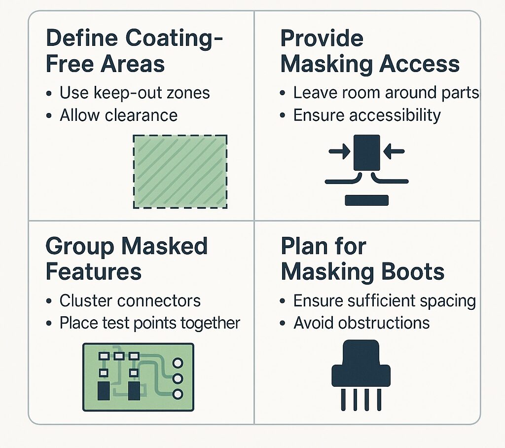
2. Define clear coating-free zones (keep-outs)
Coating-free areas protect components or surfaces that must not be coated, such as:
- Connectors and card-edge fingers
- Test points and probe pads
- High-voltage isolation paths and creepage distances
- Switches, buttons, and adjustable components
- Mechanical interfaces (screws, studs, metal frames)
Best practice rules for keep-outs
- Use a clearly defined coating keep-out zone on the mechanical or design rule layer.
- Allow typically 0.5–1.0 mm clearance around the protected feature for mask placement.
- Avoid placing small passives tight up against connector shells or card edges.
- Use copper keep-out, silkscreen, or mechanical outlines where possible for clarity.
What this prevents
- Masking tape lifting or leaking around critical features
- Parylene penetrating into connectors and mating surfaces
- Coating bridging across isolation gaps and creepage distances
- Operator-to-operator variation in masking
3. Provide adequate masking access
The number one cause of slow masking is poor physical access around features that require protection.
Allow working space around:
- Headers and I/O connectors
- Card-edge connectors and fingers
- Jumpers and links
- Tall mechanical features and brackets
- Potentiometers and trimmers
- Battery contacts
Minimum recommended access clearance
- 3–4 mm for manual tape masking
- 6+ mm for reusable masking boots
- ≥ 10 mm around tall or awkward connectors
Good access is a core part of masking access design guidelines and a major labour saver.
4. Group masking features together
Dispersed masking points increase takt time. Grouping keep-outs improves:
- Masking speed
- Consistency of coated edges
- Reduced tape usage
- Easier inspection
Cluster connectors, test points, and masked features into defined masked zones whenever practical.
5. Avoid masking nightmares in layout
Certain layout patterns repeatedly cause coating defects. Avoid:
❌ Tall components surrounded by small passives
Almost impossible to tape cleanly; promotes leakage.
❌ Deep, narrow cavities
Cause pooling, voids, and trapped air.
❌ No edge clearance around connectors
Boots cannot seal and tape cannot be applied flat.
❌ Vias too close to masking edges
Enables wicking under tape or boots.
❌ Isolation gaps hidden behind tall parts
Shadowing for spray, inconsistent Parylene coverage.
Avoiding these improves both coating quality and long-term reliability. Many of these issues also feed directly into common masking-related defects seen in production and rework.
6. Plan for reusable masking boots
Masking boots dramatically reduce labour time — but only if the PCB is designed to accept them.
To enable boot use:
- Provide at least 6 mm clearance around connectors.
- Avoid components tight to connector sides.
- Ensure unobstructed access for boot removal.
- Ensure tall components do not block boot insertion.
Boot-friendly designs cut masking time by 50–80%. Where masking difficulty has already created coating escapes, edge defects or rework, it is often worth reviewing the wider causes described in Masking Causes Most Conformal Coating Defects.
7. Consider coating process type (spray vs Parylene)
Design rules differ based on coating method.
Liquid spray coatings
- Require larger keep-outs
- Suffer from shadowing
- Need access for solvent wipe-offs
Parylene (vapour deposition)
- Penetrates every gap — seals must be perfect
- No shadowing issues, but unforgiving of poor masking
- Tolerates tight spacing but increases masking demand
8. Summary – principles of masking-friendly PCB design
- Define clear coating-free zones
- Provide mask access
- Group masked areas
- Avoid masking traps
- Enable boot use
- Align layout with coating type
Applying these principles reduces takt time and improves coating reliability.
Why Choose SCH Services?
Most masking problems are created long before coating starts. SCH Services helps customers review layout, keep-out strategy, masking access and process constraints so coating-free zones are practical to protect and repeatable to manufacture at scale.
- ✈️ Design-for-Coating Support – Practical guidance on keep-outs, masking access and feature spacing before boards reach production.
- 🛠️ Masking & Process Expertise – Support across liquid coatings, Parylene masking strategy, reusable boots and manual masking approaches.
- 📈 Reduced Labour & Rework – Recommendations focused on faster masking, lower defect risk and more repeatable coating outcomes.
- 🌍 Integrated Technical Capability – Consultancy, masking solutions, coating services, training and process troubleshooting from one specialist partner.
- ✅ Built for High-Reliability Electronics – Experience supporting demanding industrial, aerospace, defence and advanced electronics applications.
📞 Call: +44 (0)1226 249019 | ✉ Email: sales@schservices.com | 💬 Contact Us ›
