Why does cleaning improve the adhesion of the conformal coating?


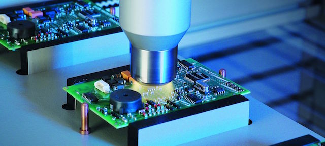
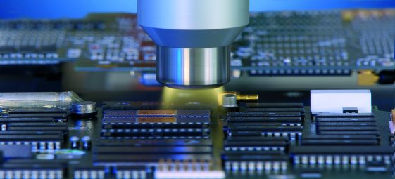
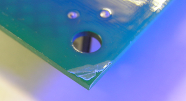
In general it is important that conformal coatings have good adhesion in order to be effective. However, there is no single theory that describes the property of adhesion for conformal coatings.

There are three basic mechanisms for conformal coatings that are known to help with good adhesion.

They are:

  1. Adsorption
  2. Chemical Bonding
  3. Mechanical Interlocking
There are three basic mechanisms for conformal coatings that are known to help with good adhesion. They are adsorption, chemical bonding and mechanical Interlocking

Adsorption

This is where the molecules in the conformal coating wet or flow freely over the substrate and make intimate contact with the substrate. This forms interfacial (electrostatic) bonds with van-der-Waal forces.

Any contamination between the two will weaken the adsorption. Any de-wetting (prevention of wetting) will also hinder the adsorption.

Cleaning the surface of contamination will help with adsorption.

Chemical bonds

The bonds are formed at the interface between the conformal coating and the substrate.

Good bonding gives strong adhesion of the conformal coating to the substrate. If bonding cannot be achieved due to contamination then poor adhesion may result.

Cleaning the surface of contamination will help the chemical bonding process.

Mechanical interlocking

The conformal coating film penetrates the roughness on the substrate surface and is achieved once the coating dries.

If the surface is smooth then the mechanical bonding is less effective. If the surface can be cleaned, leaving a rough surface, then more effective bonding can be achieved.

Cleaning the surface of contamination will help.


Achieving the best conformal coating adhesion

Surface contamination can be critical when considering conformal coating and the process. If you can clean the contamination from the surface then the adhesion of the conformal coating should improve.

All three mechanisms do not have to occur to form good adhesion. Depending on the specific conformal coating system, substrate, and application method, different mechanisms could work.

However, good wetting or adsorption is normally required for good bonding.

So, if in doubt clean the surface of the substrate to achieve good conformal coating bonding.


Need to know more about conformal coating adhesion?

Contact us now and we can discuss how we can help you.

Give us a call at (+44) 1226 249019 or email your inquiries at sales@schservices.com

What is plasma cleaning?


Plasma cleaning is a process of using plasma energy to clean and modify the surface of a substrate like a circuit board assembly.

It is a highly effective surface cleaning and treatment process before application of conformal coatings and is gaining more popularity due its highly effective performance.

Plasma cleaning is a process of using plasma energy to clean and modify the surface of a substrate like a circuit board assembly. It is a highly effective surface cleaning and treatment process before application of conformal coatings and Parylene.

What is Plasma?

Plasma is the energy-rich gas state (also known as the fourth state of matter) that can be used to modify the surface of a product to improve its performance.

Plasma technology is based on a simple physical principle.

Matter changes its state when energy is supplied to it. Solids become liquid. Liquids become gas.

If additional energy is then fed into a gas by means of electrical discharge it eventually ionises and goes into the energy-rich plasma state, plasma is created.

This modification can be improving the adhesion of a conformal coating or change the surface characteristics of the board.


How is Plasma used for improving the performance of coatings with printed circuit boards?

For electronic circuit surfaces, plasma treatment can be used in two highly effective ways.

That is it can:

  • Clean the surface of the circuit board. The surface will be free of residues and 100% contamination free including release agents and additives.
  • Activate the surface of the circuit board assembly. This will allow easier bonding and better adhesion of conformal coatings.

These properties make it an interesting technique for improving the surface performance of an electronic circuit board.

In fact, plasma treatment can clean, activate or coat nearly all surfaces. These surfaces include plastics, metals, (e.g., aluminum), glass, recycled materials and composite materials.

This means the plasma process can be highly effective on many different products.

For electronic circuits, plasma treatment can be used in two highly effective ways. First, it can clean the surface of the circuit board. Second, it can activate the surface of the circuit board assembly to allow easier bonding and better adhesion of conformal coatings and materials like Parylene.

For electronic circuits, plasma treatment can be used in two highly effective ways. First, it can clean the surface of the circuit board. Second, it can activate the surface of the circuit board assembly to allow easier bonding and better adhesion of conformal coatings and materials like Parylene.

What are the typical plasma processes available for surface treatment?

There are traditionally three types of plasma treatment:

  1. Low-pressure plasma
  2. Corona treatment
  3. Atmospheric pressure plasma

Low-pressure plasma

These plasmas are generated in closed chambers in a vacuum (10-3 to 10-9 bar).

They can be used in conjunction with Chemical Vapor Deposition (CVD) coatings like Parylene before application.

Corona treatment

Corona treatment (corona process) is a physical process involving high voltage and is mainly used for treatment of films.

This is normally not suitable for electronic circuit boards.


How is the plasma applied to a circuit board to clean and activate the surface?

For materials like liquid conformal coatings then atmospheric pressure plasma is an excellent process for cleaning surfaces and improving adhesion and surface energy performance of circuit boards for conformal coatings.

Atmospheric plasma is generated under normal pressure. This means that low-pressure chambers are not required.

The plasma is created with clean and dry compressed air and does not require forming gases. It is possible to integrate plasma directly into manufacturing processes under normal pressure conditions.

Typical plasma components used for cleaning surfaces on circuits are:

  • Plasma jets (nozzles) to apply the plasma to the surface of the circuit board. They could be controlled by a robotic system.
  • The plasma generators that create the plasma to clean or supply the coatings as required. They provide output power and, in conjunction with complete pretreatment stations, assume various control functions.
  • The process monitoring that controls the nozzles, the movement of the system and the quality of the output.

These three parts form the plasma cleaning process.

For Chemical Vapor Deposition (CVD) coatings like Parylene then low-pressure plasma can be used in the chamber before application.

These plasmas are generated in closed chambers in a vacuum (10-3 to 10-9 bar).


Want to know more about plasma cleaning and conformal coating performance?

Contact us now to discuss what we can offer you in terms of cleaning fluids from our Surclean range of materials.

Give us a call at (+44) 1226 249019 or email your inquiries at sales@schservices.com

How to clean “no clean” flux residues and get it right


Cleaning the residues left behind by a no clean flux process is one of the most difficult tasks when considering cleaning.

After all, the residues left on the circuit board are not formulated to be cleaned away easily.

How do you clean no clean flux residues if you need to?

Whether a flux residue can be cleaned effectively depends on the cleaning materials saponification factor and its compatibility with the residues.

Saponification is the ability of the no clean residues to be softened to the point of being able to be dissolved by the alkali content (the saponifier) of the cleaning chemistry. The higher the saponification factor of the cleaning fluid the easier it is to clean the residues.

So the key here is to ensure that the saponifier completely dissolves the residues.

What happens if the residues are only partially dissolved?

A no-clean residue that is only partly cleaned away may be far worse for a printed circuit board assembly (PCBA) than a no-clean residue left untouched.

One of the reasons is because lead free flux activators are more active than those in earlier leaded flux formulations.

In a no clean flux, when un-cleaned, the residues are locked up in the carrier resin matrix. They are stable (benign) at normal operational temperatures and therefore will not leach out dangerous residues and cause corrosion problems.

However, if the protective matrix around the residue is partially removed by an inadequate cleaning regime, then the activators could be exposed.

This may lead to a corrosion process starting on the circuit board. Further, this process could be accelerated in the presence of heat, power on the boards in service or high relative humidity.

So how do you clean “no-clean” residues?

It is important when considering cleaning “no-clean” residues on a circuit board that you consider three points:

  1. Can you actually clean the residue to be cleaned effectively?
  2. Have you matched the cleaning chemistry with the relative degree of difficulty and the available process?
  3. Have you validated the whole process by careful testing?

Consider these three points and it may help you be successful. Not considering these three points could easily lead you to having real problems in the long term.

Want to know more about cleaning no clean fluxes or cleaning circuit boards? 

Contact us now to discuss what we can offer you in terms of cleaning fluids from our Surclean range of materials.

Give us a call at (+44) 1226 249019 or email your inquiries at sales@schservices.com

The ABCs of Atomic Layer Deposition (ALD)


What is ALD?

Atomic Layer Deposition (ALD) belongs to the family of Chemical Vapour Deposition methods (CVD).

It is a deposition process at a nano-scale level within an enclosed vacuum chamber.

The deposition process forms ultra-thin films (atomic layers) with extremely reliable film thickness control.

This provides for highly conformal and dense films at extremely thin layers (1-100nm).

What coatings are deposited in ALD?

ALD principally deposits metal oxide ceramic films.

These films range in composition from the most basic and widely used aluminum oxide (Al2O3) and titanium oxide (TiO2) up to mixed metal oxide multilayered or doped systems.

How does ALD work in practice?

The ALD deposition technique is based upon the sequential use of a gas phase chemical process.

Gases are used to grow the films onto the substrate within a vacuum chamber.

The majority of ALD reactions use two chemicals called precursors. These precursors react with the surface of a material one at a time in a sequential, self-limiting, manner.

Through the repeated exposure to alternating gases there is a build up of a thin coating film.

Where is ALD used?

ALD is used in many different areas including:

  • Micro-electronics
  • Semiconductors
  • Photovoltaics
  • Biotechnology
  • biomedical
  • LEDs
  • Optics
  • Fuel cell systems
Advantages and disadvantages of ALD

Advantages

  • Self-Limiting. The ALD process limits the film thickness. Many other processes like Parylene are dependent upon amount of dimer and will continue to deposit successive polymer layers until it is completely used up.
  • Conformal films. ALD film thickness can be uniform from end to end throughout the chamber. Other coatings like Parylene can have a varied coating thickness across the chamber and the devices being coated.
  • Pinhole free. ALD films can be pinhole-free at a sub-nanometer thickness. Parylene and some other materials are only pinhole-free at micron levels.
  • ALD allows layers or laminates. Most other films including Parylene are single component layers.

Disadvantages

  • High purity substrate. This is very important to the quality of the finish similar to many other vapour deposition processes.
  • ALD Systems can range anywhere from $200,000 to $800,000 based on the quality and efficiency of the instrument. This tends to be 3-4 times the prices of a Parylene system.
  • Reaction time. Traditionally, the process of ALD is very slow and this is known to be its major limitation.
  • Masking challenges. The ALD masking process must be perfect. Any pinhole in the masking process will allow deposition beyond the masking barrier.
What are some of the ALD coatings that can be deposited?

A wide variety of chemistries are possible with Atomic Layer Deposition.

They include:

  • Oxides
  • Nitrides
  • Metals
  • Carbides
  • Sulfides

Want to know more about Atomic Layer Deposition (ALD) coatings?

Contact us now!

Call us on +44 (0) 1226 249019, email your requirements on sales@schservices.com

Introducing a new coating that could offer the ultimate protection for LEDs without compromise to performance or process cost


The need to protect LEDs from the long –term exposure of a harsh environment is becoming more and more required. This is doubly so for LEDs used outdoors.

The alternative coatings used to protect LEDs are many. They include Parylene, conformal coatings, ultra-thin fluoropolymer materials and encapsulates.

However, none of the material processes offer the perfect protection without adding significant cost to the production process, and ultimately the circuit board and product.

Further, to reduce costs in production some of the coating materials used compromised performance. So, there is a typical balance of costs versus protection.

Now, this may all change with the introduction of a very new coating process that takes many of the performance benefits of the best coatings but does not suffer the associated problems of increased production costs.

This process is a hybrid ALD (Atomic Layer Deposition)/CVD (Chemical Vapor Deposition) technique.

So what is a Hybrid ALD / CVD technique?

Most people in conformal coating have heard of Parylene. Parylene is a CVD (chemical vapor deposition) process where the Parylene material is applied in a vacuum chamber and the coating builds up on the surface of the circuit.

The new hybrid process uses CVD as one of its film processes. However, how it differs is that the method also uses another technique, ALD (atomic layer deposition).

Further, these two processes, ALD and CVD are applied sequentially. They are deposited as ultra-thin coatings (nanometer scale thickness) one on top of the other.

This build up of multiple layers of ultra-thin coatings (alternating ALD and CVD films) with differing coating properties produces a completely different hybrid coating that outperforms the individual coatings produced by ALD and CVD alone.

Further, the final layer applied is a hydrophobic barrier that further enhances the performance of the coating.

So how does the hybrid film differ to traditional materials like Parylene and liquid conformal coatings for protecting LEDs?

First, the hybrid coatings protective performance has been found to be superior to them all in most categories of testing so far. It provides both improved electrical and physical properties that protect the circuits.

A major issue for LEDs is light loss when the film is applied over the LEDs. For the hybrid coating the coating shows zero loss of light and this is a great advantage.

Also, the material is both temperature and UV stable. The coating will survive up to 350C and does not degrade in UV light. Again, these are great advantages for the performance of the hybrid coating.

It is also hydrophobic. This property rejects water from the surface and improves the film properties enormously.

However, what makes this coating exceptional is its final property. That is the coating does not require the circuit board to be masked when the coating is being applied!

So, why does the hybrid film not need masking like other traditional conformal coatings and Parylene?

The difference is film thickness.

The hybrid film is much thinner than the other traditional coatings including Parylene. Typical film thicknesses can be as low as 0.1um.

Since the coating is extremely thin (<< less than traditional coatings) then it has been found that no masking is required.

This is because when components like connectors are joined together then the ultrathin coating does not prevent electrical connection. The component mating parts connect together and no loss of connection can be measured.

Even better, the physical protection of the film is not compromised. In fact, all of the components including connectors are protected.

This means that the cost of process is purely the cost of application of the material and nothing else.

Since the process is relatively low cost then this does offer a very interesting alternative to the traditional coating materials in LED processing.

Doesn’t the hybrid ALD / CVD process sound complex to operate?

Actually, although the technology and chemistry can be a little complex the process itself is fairly simple.

Once the process is set up in the machine the operator just loads, switches the machine on, waits for the coating to be applied and unloads on completion.  

This is a far cry from the sophisticated processes of robotic selective coating or the challenges of Parylene. Further, the application process is actually very stable and in reality is tried and test in other industries for a long time.

So, how well did the hybrid coating perform in protecting the LEDs?

Nexus, an online conformal coating database, actually worked with live LED circuits from a customer and tested the hybrid ALD / CVD material.

The customer LED product was an outdoor application. The LED customer used their own in-house test methods to prove the technology.

As part of the testing the LED circuit was exposed to tests for resistance against salt, moisture and temperature.

The test methods included:

  • Initial test submerged in DI water dip for 12 hours
  • Second test submerged in 25% concentration saltwater dip for 17 hours
  • Third test 2 x 6 hour cycles in water ramped from room temperature to 70°C

After each test the boards were tested for failure or problems.

The LED circuit passed on all tests. All results achieved were completed with no masking of components and zero light loss in LED opacity.

The electrical connections were found to be excellent and the coating did not affect the integrity of the connectors.

So what about the cost of process?

Since the hybrid film process is masking and de-masking free then the cost per unit is incredibly low. This makes the material superior to nearly all the traditional methods of coating protection.

Further, the protective properties of the hybrid coating in nearly all cases is superior to the conventional methods.

So, you get a lower cost coating with a higher technical performance.

So, just how good is the hybrid ALD / CVD coating as a protective material for electronics?

Generally, with protective coatings for electronics then Parylene is considered the gold standard in most cases.

So, Nexus compared Parylene with the hybrid ALD / CVD material.


Property Parylene ALD/CVD Coating
Hardness Soft Hard
Wear resistance/Handling Ease Poor Excellent
Water Vapor Transmission Rate Good Excellent
Temperature Resistance (extended time) 100°C 350°C
Color Gray/white Clear
Adhesion to various materials Poor Excellent
Scalable to large production Poor Excellent
Process Time 8 – 12 hrs 8 – 12 hrs
Hydrophobicity Good Good – Excellent
Cost High Low – Med

Table courtesy of Nexus

What Nexus also identified for the material were some key properties for LEDs.

  • The Water Vapor Transmission Rate (WVTR) is superior to Parylene so the coating is far more waterproof for the LEDs
  • Coating adhesion is superior as it covalently bonds to the substrate. So, the lifetime of the material will be better on the circuit.
  • The hybrid coating is UV stable whereas Parylene in general is not. This is an important criteria for coatings exposed outside on LEDs
  • The coating stayed 100% transparent during testing (no loss of lux). That again is important for LEDs.
  • The coating thickness of the hybrid material is x10 LESS than the Parylene. This aids light transmission and electric connectivity
  • The film is hydrophobic so repels water and aids the performance of the coating.

So, in reality the hybrid ALD / CVD material could just be what the LED industry is looking for in protecting their circuits.

Nexus will be performing further tests on the material to see how it performs on other types of circuits shortly.

Need to find out more?

For further information on the hybrid ALD / CVD materials then contact us directly. We can help you trial the coating.

Or, check out the Nexus article, Coating LEDs with a hybrid ALD / CVD Process.

Call us on +44 (0) 1226 249019, email your requirements on sales@schservices.com

0
    0
    Your Cart
    Your cart is empty
      Calculate Shipping